 Add to Chrome
 Add to Firefox
 Add to Edge
AI+HW 2035: Shaping the Next Decade
Mar 05, 2026Artificial intelligence (AI) and hardware (HW) are advancing at unprecedented rates, yet their trajectories have become inseparably intertwined. The global research community lacks a cohesive, long-term vision to strategically coordinate the development of AI and HW. This fragmentation constrains progress toward holistic, sustainable, and adaptive AI systems capable of learning, reasoning, and operating efficiently across cloud, edge, and physical environments. The future of AI depends not only on scaling intelligence, but on scaling efficiency, achieving exponential gains in intelligence per joule, rather than unbounded compute consumption. Addressing this grand challenge requires rethinking the entire computing stack. This vision paper lays out a 10-year roadmap for AI+HW co-design and co-development, spanning algorithms, architectures, systems, and sustainability. We articulate key insights that redefine scaling around energy efficiency, system-level integration, and cross-layer optimization. We identify key challenges and opportunities, candidly assess potential obstacles and pitfalls, and propose integrated solutions grounded in algorithmic innovation, hardware advances, and software abstraction. Looking ahead, we define what success means in 10 years: achieving a 1000x improvement in efficiency for AI training and inference; enabling energy-aware, self-optimizing systems that seamlessly span cloud, edge, and physical AI; democratizing access to advanced AI infrastructure; and embedding human-centric principles into the design of intelligent systems. Finally, we outline concrete action items for academia, industry, government, and the broader community, calling for coordinated national initiatives, shared infrastructure, workforce development, cross-agency collaboration, and sustained public-private partnerships to ensure that AI+HW co-design becomes a unifying long-term mission.
Report for NSF Workshop on AI for Electronic Design Automation
Jan 20, 2026This report distills the discussions and recommendations from the NSF Workshop on AI for Electronic Design Automation (EDA), held on December 10, 2024 in Vancouver alongside NeurIPS 2024. Bringing together experts across machine learning and EDA, the workshop examined how AI-spanning large language models (LLMs), graph neural networks (GNNs), reinforcement learning (RL), neurosymbolic methods, etc.-can facilitate EDA and shorten design turnaround. The workshop includes four themes: (1) AI for physical synthesis and design for manufacturing (DFM), discussing challenges in physical manufacturing process and potential AI applications; (2) AI for high-level and logic-level synthesis (HLS/LLS), covering pragma insertion, program transformation, RTL code generation, etc.; (3) AI toolbox for optimization and design, discussing frontier AI developments that could potentially be applied to EDA tasks; and (4) AI for test and verification, including LLM-assisted verification tools, ML-augmented SAT solving, security/reliability challenges, etc. The report recommends NSF to foster AI/EDA collaboration, invest in foundational AI for EDA, develop robust data infrastructures, promote scalable compute infrastructure, and invest in workforce development to democratize hardware design and enable next-generation hardware systems. The workshop information can be found on the website https://ai4eda-workshop.github.io/.
Hyperdimensional Computing Nanosystem
Nov 23, 2018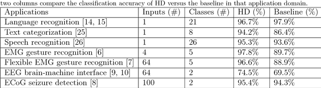
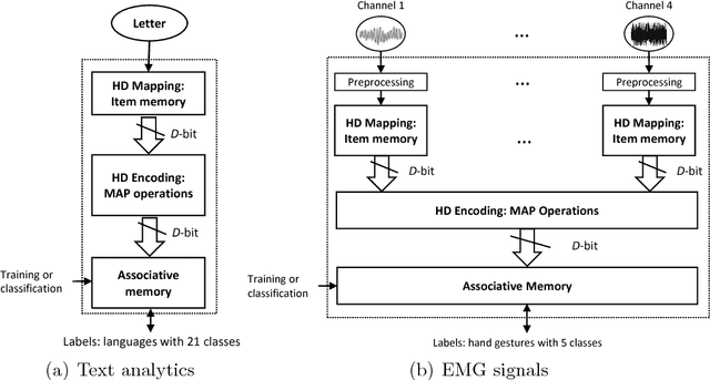
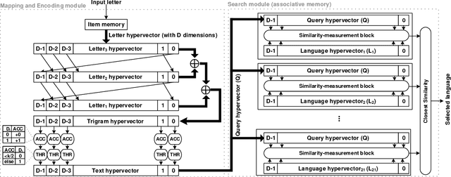
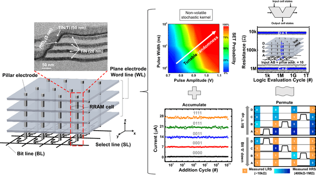
One viable solution for continuous reduction in energy-per-operation is to rethink functionality to cope with uncertainty by adopting computational approaches that are inherently robust to uncertainty. It requires a novel look at data representations, associated operations, and circuits, and at materials and substrates that enable them. 3D integrated nanotechnologies combined with novel brain-inspired computational paradigms that support fast learning and fault tolerance could lead the way. Recognizing the very size of the brain's circuits, hyperdimensional (HD) computing can model neural activity patterns with points in a HD space, that is, with hypervectors as large randomly generated patterns. At its very core, HD computing is about manipulating and comparing these patterns inside memory. Emerging nanotechnologies such as carbon nanotube field effect transistors (CNFETs) and resistive RAM (RRAM), and their monolithic 3D integration offer opportunities for hardware implementations of HD computing through tight integration of logic and memory, energy-efficient computation, and unique device characteristics. We experimentally demonstrate and characterize an end-to-end HD computing nanosystem built using monolithic 3D integration of CNFETs and RRAM. With our nanosystem, we experimentally demonstrate classification of 21 languages with measured accuracy of up to 98% on >20,000 sentences (6.4 million characters), training using one text sample (~100,000 characters) per language, and resilient operation (98% accuracy) despite 78% hardware errors in HD representation (outputs stuck at 0 or 1). By exploiting the unique properties of the underlying nanotechnologies, we show that HD computing, when implemented with monolithic 3D integration, can be up to 420X more energy-efficient while using 25X less area compared to traditional silicon CMOS implementations.