 Add to Chrome
 Add to Firefox
 Add to Edge
CrossNAS: A Cross-Layer Neural Architecture Search Framework for PIM Systems
May 28, 2025In this paper, we propose the CrossNAS framework, an automated approach for exploring a vast, multidimensional search space that spans various design abstraction layers-circuits, architecture, and systems-to optimize the deployment of machine learning workloads on analog processing-in-memory (PIM) systems. CrossNAS leverages the single-path one-shot weight-sharing strategy combined with the evolutionary search for the first time in the context of PIM system mapping and optimization. CrossNAS sets a new benchmark for PIM neural architecture search (NAS), outperforming previous methods in both accuracy and energy efficiency while maintaining comparable or shorter search times.
NSF-MAP: Neurosymbolic Multimodal Fusion for Robust and Interpretable Anomaly Prediction in Assembly Pipelines
May 09, 2025In modern assembly pipelines, identifying anomalies is crucial in ensuring product quality and operational efficiency. Conventional single-modality methods fail to capture the intricate relationships required for precise anomaly prediction in complex predictive environments with abundant data and multiple modalities. This paper proposes a neurosymbolic AI and fusion-based approach for multimodal anomaly prediction in assembly pipelines. We introduce a time series and image-based fusion model that leverages decision-level fusion techniques. Our research builds upon three primary novel approaches in multimodal learning: time series and image-based decision-level fusion modeling, transfer learning for fusion, and knowledge-infused learning. We evaluate the novel method using our derived and publicly available multimodal dataset and conduct comprehensive ablation studies to assess the impact of our preprocessing techniques and fusion model compared to traditional baselines. The results demonstrate that a neurosymbolic AI-based fusion approach that uses transfer learning can effectively harness the complementary strengths of time series and image data, offering a robust and interpretable approach for anomaly prediction in assembly pipelines with enhanced performance. \noindent The datasets, codes to reproduce the results, supplementary materials, and demo are available at https://github.com/ChathurangiShyalika/NSF-MAP.
LLMPi: Optimizing LLMs for High-Throughput on Raspberry Pi
Apr 02, 2025Deploying Large Language Models (LLMs) on resource-constrained edge devices like the Raspberry Pi presents challenges in computational efficiency, power consumption, and response latency. This paper explores quantization-based optimization techniques to enable high-throughput, energy-efficient execution of LLMs on low-power embedded systems. Our approach leverages k-quantization, a Post-Training Quantization (PTQ) method designed for different bit-widths, enabling efficient 2-bit, 4-bit, 6-bit, and 8-bit weight quantization. Additionally, we employ ternary quantization using Quantization-Aware Training (QAT) for BitNet models, allowing for more effective adaptation to lower-bit representations while preserving accuracy. Our findings highlight the potential of quantized LLMs for real-time conversational AI on edge devices, paving the way for low-power, high-efficiency AI deployment in mobile and embedded applications. This study demonstrates that aggressive quantization strategies can significantly reduce energy consumption while maintaining inference quality, making LLMs practical for resource-limited environments.
PIM-LLM: A High-Throughput Hybrid PIM Architecture for 1-bit LLMs
Mar 31, 2025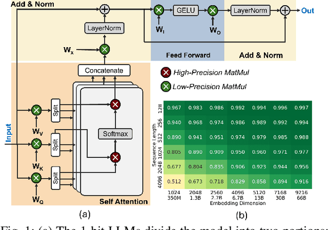
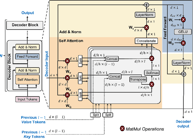
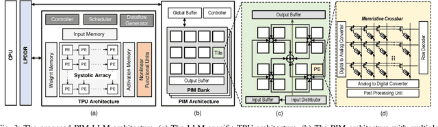
In this paper, we propose PIM-LLM, a hybrid architecture developed to accelerate 1-bit large language models (LLMs). PIM-LLM leverages analog processing-in-memory (PIM) architectures and digital systolic arrays to accelerate low-precision matrix multiplication (MatMul) operations in projection layers and high-precision MatMul operations in attention heads of 1-bit LLMs, respectively. Our design achieves up to roughly 80x improvement in tokens per second and a 70% increase in tokens per joule compared to conventional hardware accelerators. Additionally, PIM-LLM outperforms previous PIM-based LLM accelerators, setting a new benchmark with at least 2x and 5x improvement in GOPS and GOPS/W, respectively.
TPU-Gen: LLM-Driven Custom Tensor Processing Unit Generator
Mar 07, 2025The increasing complexity and scale of Deep Neural Networks (DNNs) necessitate specialized tensor accelerators, such as Tensor Processing Units (TPUs), to meet various computational and energy efficiency requirements. Nevertheless, designing optimal TPU remains challenging due to the high domain expertise level, considerable manual design time, and lack of high-quality, domain-specific datasets. This paper introduces TPU-Gen, the first Large Language Model (LLM) based framework designed to automate the exact and approximate TPU generation process, focusing on systolic array architectures. TPU-Gen is supported with a meticulously curated, comprehensive, and open-source dataset that covers a wide range of spatial array designs and approximate multiply-and-accumulate units, enabling design reuse, adaptation, and customization for different DNN workloads. The proposed framework leverages Retrieval-Augmented Generation (RAG) as an effective solution for a data-scare hardware domain in building LLMs, addressing the most intriguing issue, hallucinations. TPU-Gen transforms high-level architectural specifications into optimized low-level implementations through an effective hardware generation pipeline. Our extensive experimental evaluations demonstrate superior performance, power, and area efficiency, with an average reduction in area and power of 92\% and 96\% from the manual optimization reference values. These results set new standards for driving advancements in next-generation design automation tools powered by LLMs.
AssemAI: Interpretable Image-Based Anomaly Detection for Manufacturing Pipelines
Aug 05, 2024


Anomaly detection in manufacturing pipelines remains a critical challenge, intensified by the complexity and variability of industrial environments. This paper introduces AssemAI, an interpretable image-based anomaly detection system tailored for smart manufacturing pipelines. Our primary contributions include the creation of a tailored image dataset and the development of a custom object detection model, YOLO-FF, designed explicitly for anomaly detection in manufacturing assembly environments. Utilizing the preprocessed image dataset derived from an industry-focused rocket assembly pipeline, we address the challenge of imbalanced image data and demonstrate the importance of image-based methods in anomaly detection. The proposed approach leverages domain knowledge in data preparation, model development and reasoning. We compare our method against several baselines, including simple CNN and custom Visual Transformer (ViT) models, showcasing the effectiveness of our custom data preparation and pretrained CNN integration. Additionally, we incorporate explainability techniques at both user and model levels, utilizing ontology for user-friendly explanations and SCORE-CAM for in-depth feature and model analysis. Finally, the model was also deployed in a real-time setting. Our results include ablation studies on the baselines, providing a comprehensive evaluation of the proposed system. This work highlights the broader impact of advanced image-based anomaly detection in enhancing the reliability and efficiency of smart manufacturing processes.
HiRISE: High-Resolution Image Scaling for Edge ML via In-Sensor Compression and Selective ROI
Jul 23, 2024


With the rise of tiny IoT devices powered by machine learning (ML), many researchers have directed their focus toward compressing models to fit on tiny edge devices. Recent works have achieved remarkable success in compressing ML models for object detection and image classification on microcontrollers with small memory, e.g., 512kB SRAM. However, there remain many challenges prohibiting the deployment of ML systems that require high-resolution images. Due to fundamental limits in memory capacity for tiny IoT devices, it may be physically impossible to store large images without external hardware. To this end, we propose a high-resolution image scaling system for edge ML, called HiRISE, which is equipped with selective region-of-interest (ROI) capability leveraging analog in-sensor image scaling. Our methodology not only significantly reduces the peak memory requirements, but also achieves up to 17.7x reduction in data transfer and energy consumption.
Towards Efficient Deployment of Hybrid SNNs on Neuromorphic and Edge AI Hardware
Jul 11, 2024


This paper explores the synergistic potential of neuromorphic and edge computing to create a versatile machine learning (ML) system tailored for processing data captured by dynamic vision sensors. We construct and train hybrid models, blending spiking neural networks (SNNs) and artificial neural networks (ANNs) using PyTorch and Lava frameworks. Our hybrid architecture integrates an SNN for temporal feature extraction and an ANN for classification. We delve into the challenges of deploying such hybrid structures on hardware. Specifically, we deploy individual components on Intel's Neuromorphic Processor Loihi (for SNN) and Jetson Nano (for ANN). We also propose an accumulator circuit to transfer data from the spiking to the non-spiking domain. Furthermore, we conduct comprehensive performance analyses of hybrid SNN-ANN models on a heterogeneous system of neuromorphic and edge AI hardware, evaluating accuracy, latency, power, and energy consumption. Our findings demonstrate that the hybrid spiking networks surpass the baseline ANN model across all metrics and outperform the baseline SNN model in accuracy and latency.
Flex-TPU: A Flexible TPU with Runtime Reconfigurable Dataflow Architecture
Jul 11, 2024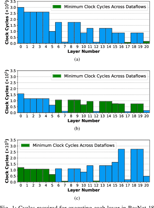
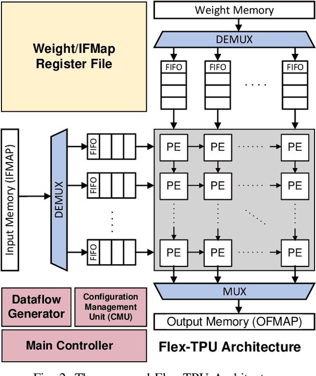
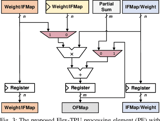
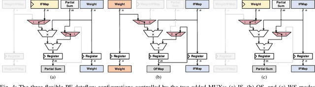
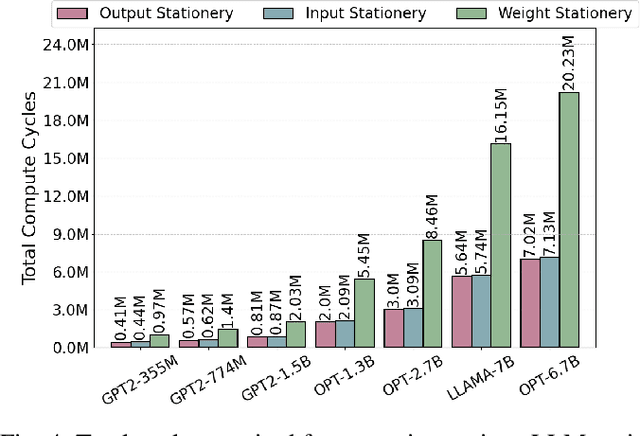
Tensor processing units (TPUs) are one of the most well-known machine learning (ML) accelerators utilized at large scale in data centers as well as in tiny ML applications. TPUs offer several improvements and advantages over conventional ML accelerators, like graphical processing units (GPUs), being designed specifically to perform the multiply-accumulate (MAC) operations required in the matrix-matrix and matrix-vector multiplies extensively present throughout the execution of deep neural networks (DNNs). Such improvements include maximizing data reuse and minimizing data transfer by leveraging the temporal dataflow paradigms provided by the systolic array architecture. While this design provides a significant performance benefit, the current implementations are restricted to a single dataflow consisting of either input, output, or weight stationary architectures. This can limit the achievable performance of DNN inference and reduce the utilization of compute units. Therefore, the work herein consists of developing a reconfigurable dataflow TPU, called the Flex-TPU, which can dynamically change the dataflow per layer during run-time. Our experiments thoroughly test the viability of the Flex-TPU comparing it to conventional TPU designs across multiple well-known ML workloads. The results show that our Flex-TPU design achieves a significant performance increase of up to 2.75x compared to conventional TPU, with only minor area and power overheads.
Lightator: An Optical Near-Sensor Accelerator with Compressive Acquisition Enabling Versatile Image Processing
Mar 08, 2024


This paper proposes a high-performance and energy-efficient optical near-sensor accelerator for vision applications, called Lightator. Harnessing the promising efficiency offered by photonic devices, Lightator features innovative compressive acquisition of input frames and fine-grained convolution operations for low-power and versatile image processing at the edge for the first time. This will substantially diminish the energy consumption and latency of conversion, transmission, and processing within the established cloud-centric architecture as well as recently designed edge accelerators. Our device-to-architecture simulation results show that with favorable accuracy, Lightator achieves 84.4 Kilo FPS/W and reduces power consumption by a factor of ~24x and 73x on average compared with existing photonic accelerators and GPU baseline.