 Add to Chrome
 Add to Firefox
 Add to Edge
Neuromorphic Spiking Ring Attractor for Proprioceptive Joint-State Estimation
Apr 15, 2026Maintaining stable internal representations of continuous variables is fundamental for effective robotic control. Continuous attractor networks provide a biologically inspired mechanism for encoding such variables, yet neuromorphic realizations have rarely addressed proprioceptive estimation under resource constraints. This work introduces a spiking ring-attractor network representing a robot joint angle through self-sustaining population activity. Local excitation and broad inhibition support a stable activity bump, while velocity-modulated asymmetries drive its translation and boundary conditions confine motion within mechanical limits. The network reproduces smooth trajectory tracking and remains stable near joint limits, showing reduced drift and improved accuracy compared to unbounded models. Such compact hardware-compatible implementation preserves multi-second stability demonstrating a near-linear relationship between bump velocity and synaptic modulation.
Mixed-signal implementation of feedback-control optimizer for single-layer Spiking Neural Networks
Mar 25, 2026On-chip learning is key to scalable and adaptive neuromorphic systems, yet existing training methods are either difficult to implement in hardware or overly restrictive. However, recent studies show that feedback-control optimizers can enable expressive, on-chip training of neuromorphic devices. In this work, we present a proof-of-concept implementation of such feedback-control optimizers on a mixed-signal neuromorphic processor. We assess the proposed approach in an In-The-Loop(ITL) training setup on both a binary classification task and the nonlinear Yin-Yang problem, demonstrating on-chip training that matches the performance of numerical simulations and gradient-based baselines. Our results highlight the feasibility of feedback-driven, online learning under realistic mixed-signal constraints, and represent a co-design approach toward embedding such rules directly in silicon for autonomous and adaptive neuromorphic computing.
DendroNN: Dendrocentric Neural Networks for Energy-Efficient Classification of Event-Based Data
Mar 10, 2026Spatiotemporal information is at the core of diverse sensory processing and computational tasks. Feed-forward spiking neural networks can be used to solve these tasks while offering potential benefits in terms of energy efficiency by computing event-based. However, they have trouble decoding temporal information with high accuracy. Thus, they commonly resort to recurrence or delays to enhance their temporal computing ability which, however, bring downsides in terms of hardware-efficiency. In the brain, dendrites are computational powerhouses that just recently started to be acknowledged in such machine learning systems. In this work, we focus on a sequence detection mechanism present in branches of dendrites and translate it into a novel type of neural network by introducing a dendrocentric neural network, DendroNN. DendroNNs identify unique incoming spike sequences as spatiotemporal features. This work further introduces a rewiring phase to train the non-differentiable spike sequences without the use of gradients. During the rewiring, the network memorizes frequently occurring sequences and additionally discards those that do not contribute any discriminative information. The networks display competitive accuracies across various event-based time series datasets. We also propose an asynchronous digital hardware architecture using a time-wheel mechanism that builds on the event-driven design of DendroNNs, eliminating per-step global updates typical of delay- or recurrence-based models. By leveraging a DendroNN's dynamic and static sparsity along with intrinsic quantization, it achieves up to 4x higher efficiency than state-of-the-art neuromorphic hardware at comparable accuracy on the same audio classification task, demonstrating its suitability for spatiotemporal event-based computing. This work offers a novel approach to low-power spatiotemporal processing on event-driven hardware.
Training slow silicon neurons to control extremely fast robots with spiking reinforcement learning
Jan 29, 2026Air hockey demands split-second decisions at high puck velocities, a challenge we address with a compact network of spiking neurons running on a mixed-signal analog/digital neuromorphic processor. By co-designing hardware and learning algorithms, we train the system to achieve successful puck interactions through reinforcement learning in a remarkably small number of trials. The network leverages fixed random connectivity to capture the task's temporal structure and adopts a local e-prop learning rule in the readout layer to exploit event-driven activity for fast and efficient learning. The result is real-time learning with a setup comprising a computer and the neuromorphic chip in-the-loop, enabling practical training of spiking neural networks for robotic autonomous systems. This work bridges neuroscience-inspired hardware with real-world robotic control, showing that brain-inspired approaches can tackle fast-paced interaction tasks while supporting always-on learning in intelligent machines.
ElfCore: A 28nm Neural Processor Enabling Dynamic Structured Sparse Training and Online Self-Supervised Learning with Activity-Dependent Weight Update
Dec 24, 2025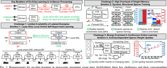
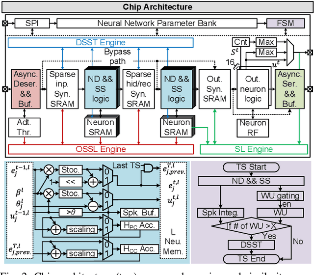
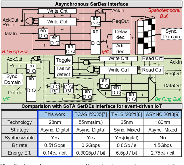
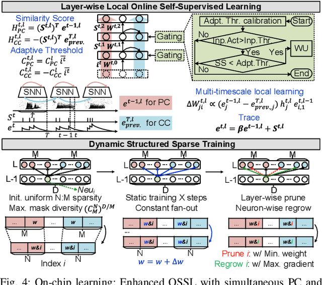
In this paper, we present ElfCore, a 28nm digital spiking neural network processor tailored for event-driven sensory signal processing. ElfCore is the first to efficiently integrate: (1) a local online self-supervised learning engine that enables multi-layer temporal learning without labeled inputs; (2) a dynamic structured sparse training engine that supports high-accuracy sparse-to-sparse learning; and (3) an activity-dependent sparse weight update mechanism that selectively updates weights based solely on input activity and network dynamics. Demonstrated on tasks including gesture recognition, speech, and biomedical signal processing, ElfCore outperforms state-of-the-art solutions with up to 16X lower power consumption, 3.8X reduced on-chip memory requirements, and 5.9X greater network capacity efficiency.
* This paper has been published in the proceedings of the 2025 IEEE European Solid-State Electronics Research Conference (ESSERC)
Algorithm-hardware co-design of neuromorphic networks with dual memory pathways
Dec 11, 2025Spiking neural networks excel at event-driven sensing. Yet, maintaining task-relevant context over long timescales both algorithmically and in hardware, while respecting both tight energy and memory budgets, remains a core challenge in the field. We address this challenge through novel algorithm-hardware co-design effort. At the algorithm level, inspired by the cortical fast-slow organization in the brain, we introduce a neural network with an explicit slow memory pathway that, combined with fast spiking activity, enables a dual memory pathway (DMP) architecture in which each layer maintains a compact low-dimensional state that summarizes recent activity and modulates spiking dynamics. This explicit memory stabilizes learning while preserving event-driven sparsity, achieving competitive accuracy on long-sequence benchmarks with 40-60% fewer parameters than equivalent state-of-the-art spiking neural networks. At the hardware level, we introduce a near-memory-compute architecture that fully leverages the advantages of the DMP architecture by retaining its compact shared state while optimizing dataflow, across heterogeneous sparse-spike and dense-memory pathways. We show experimental results that demonstrate more than a 4x increase in throughput and over a 5x improvement in energy efficiency compared with state-of-the-art implementations. Together, these contributions demonstrate that biological principles can guide functional abstractions that are both algorithmically effective and hardware-efficient, establishing a scalable co-design paradigm for real-time neuromorphic computation and learning.
A neuromorphic continuous soil monitoring system for precision irrigation
Sep 17, 2025Sensory processing at the edge requires ultra-low power stand-alone computing technologies. This is particularly true for modern agriculture and precision irrigation systems which aim to optimize water usage by monitoring key environmental observables continuously using distributed efficient embedded processing elements. Neuromorphic processing systems are emerging as a promising technology for extreme edge-computing applications that need to run on resource-constrained hardware. As such, they are a very good candidate for implementing efficient water management systems based on data measured from soil and plants, across large fields. In this work, we present a fully energy-efficient neuromorphic irrigation control system that operates autonomously without any need for data transmission or remote processing. Leveraging the properties of a biologically realistic spiking neural network, our system performs computation, and decision-making locally. We validate this approach using real-world soil moisture data from apple and kiwi orchards applied to a mixed-signal neuromorphic processor, and show that the generated irrigation commands closely match those derived from conventional methods across different soil depths. Our results show that local neuromorphic inference can maintain decision accuracy, paving the way for autonomous, sustainable irrigation solutions at scale.
Spiking Neural Network Decoders of Finger Forces from High-Density Intramuscular Microelectrode Arrays
Sep 04, 2025


Restoring naturalistic finger control in assistive technologies requires the continuous decoding of motor intent with high accuracy, efficiency, and robustness. Here, we present a spike-based decoding framework that integrates spiking neural networks (SNNs) with motor unit activity extracted from high-density intramuscular microelectrode arrays. We demonstrate simultaneous and proportional decoding of individual finger forces from motor unit spike trains during isometric contractions at 15% of maximum voluntary contraction using SNNs. We systematically evaluated alternative SNN decoder configurations and compared two possible input modalities: physiologically grounded motor unit spike trains and spike-encoded intramuscular EMG signals. Through this comparison, we quantified trade-offs between decoding accuracy, memory footprint, and robustness to input errors. The results showed that shallow SNNs can reliably decode finger-level motor intent with competitive accuracy and minimal latency, while operating with reduced memory requirements and without the need for external preprocessing buffers. This work provides a practical blueprint for integrating SNNs into finger-level force decoding systems, demonstrating how the choice of input representation can be strategically tailored to meet application-specific requirements for accuracy, robustness, and memory efficiency.
Waves and symbols in neuromorphic hardware: from analog signal processing to digital computing on the same computational substrate
Feb 27, 2025Neural systems use the same underlying computational substrate to carry out analog filtering and signal processing operations, as well as discrete symbol manipulation and digital computation. Inspired by the computational principles of canonical cortical microcircuits, we propose a framework for using recurrent spiking neural networks to seamlessly and robustly switch between analog signal processing and categorical and discrete computation. We provide theoretical analysis and practical neural network design tools to formally determine the conditions for inducing this switch. We demonstrate the robustness of this framework experimentally with hardware soft Winner-Take-All and mixed-feedback recurrent spiking neural networks, implemented by appropriately configuring the analog neuron and synapse circuits of a mixed-signal neuromorphic processor chip.
An Efficient Multicast Addressing Encoding Scheme for Multi-Core Neuromorphic Processors
Nov 18, 2024Multi-core neuromorphic processors are becoming increasingly significant due to their energy-efficient local computing and scalable modular architecture, particularly for event-based processing applications. However, minimizing the cost of inter-core communication, which accounts for the majority of energy usage, remains a challenging issue. Beyond optimizing circuit design at lower abstraction levels, an efficient multicast addressing scheme is crucial. We propose a hierarchical bit string encoding scheme that largely expands the addressing capability of state-of-the-art symbol-based schemes for the same number of routing bits. When put at work with a real neuromorphic task, this hierarchical bit string encoding achieves a reduction in area cost by approximately 29% and decreases energy consumption by about 50%.