 Add to Chrome
 Add to Firefox
 Add to Edge
Solder inspection
Papers and Code
Detecting Manufacturing Defects in PCBs via Data-Centric Machine Learning on Solder Paste Inspection Features
Sep 06, 2023


Automated detection of defects in Printed Circuit Board (PCB) manufacturing using Solder Paste Inspection (SPI) and Automated Optical Inspection (AOI) machines can help improve operational efficiency and significantly reduce the need for manual intervention. In this paper, using SPI-extracted features of 6 million pins, we demonstrate a data-centric approach to train Machine Learning (ML) models to detect PCB defects at three stages of PCB manufacturing. The 6 million PCB pins correspond to 2 million components that belong to 15,387 PCBs. Using a base extreme gradient boosting (XGBoost) ML model, we iterate on the data pre-processing step to improve detection performance. Combining pin-level SPI features using component and PCB IDs, we developed training instances also at the component and PCB level. This allows the ML model to capture any inter-pin, inter-component, or spatial effects that may not be apparent at the pin level. Models are trained at the pin, component, and PCB levels, and the detection results from the different models are combined to identify defective components.
SolderNet: Towards Trustworthy Visual Inspection of Solder Joints in Electronics Manufacturing Using Explainable Artificial Intelligence
Nov 18, 2022In electronics manufacturing, solder joint defects are a common problem affecting a variety of printed circuit board components. To identify and correct solder joint defects, the solder joints on a circuit board are typically inspected manually by trained human inspectors, which is a very time-consuming and error-prone process. To improve both inspection efficiency and accuracy, in this work we describe an explainable deep learning-based visual quality inspection system tailored for visual inspection of solder joints in electronics manufacturing environments. At the core of this system is an explainable solder joint defect identification system called SolderNet which we design and implement with trust and transparency in mind. While several challenges remain before the full system can be developed and deployed, this study presents important progress towards trustworthy visual inspection of solder joints in electronics manufacturing.
Fine-grained Classification of Solder Joints with α-skew Jensen-Shannon Divergence
Sep 20, 2022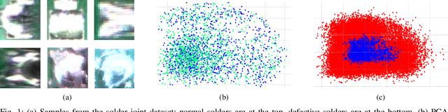
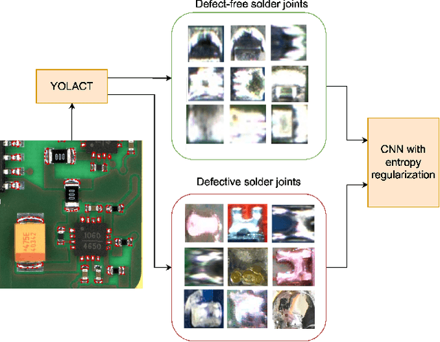
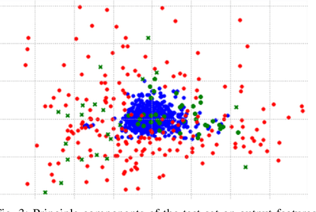
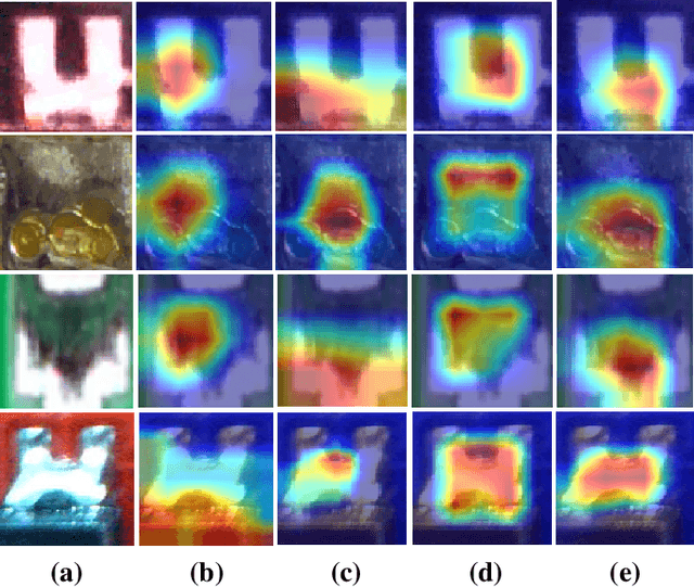
Solder joint inspection (SJI) is a critical process in the production of printed circuit boards (PCB). Detection of solder errors during SJI is quite challenging as the solder joints have very small sizes and can take various shapes. In this study, we first show that solders have low feature diversity, and that the SJI can be carried out as a fine-grained image classification task which focuses on hard-to-distinguish object classes. To improve the fine-grained classification accuracy, penalizing confident model predictions by maximizing entropy was found useful in the literature. Inline with this information, we propose using the {\alpha}-skew Jensen-Shannon divergence ({\alpha}-JS) for penalizing the confidence in model predictions. We compare the {\alpha}-JS regularization with both existing entropyregularization based methods and the methods based on attention mechanism, segmentation techniques, transformer models, and specific loss functions for fine-grained image classification tasks. We show that the proposed approach achieves the highest F1-score and competitive accuracy for different models in the finegrained solder joint classification task. Finally, we visualize the activation maps and show that with entropy-regularization, more precise class-discriminative regions are localized, which are also more resilient to noise. Code will be made available here upon acceptance.
ChangeChip: A Reference-Based Unsupervised Change Detection for PCB Defect Detection
Sep 13, 2021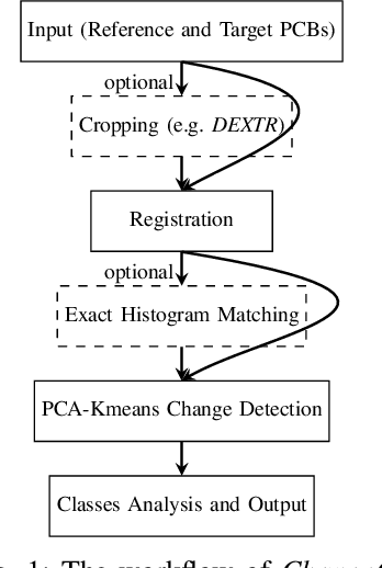
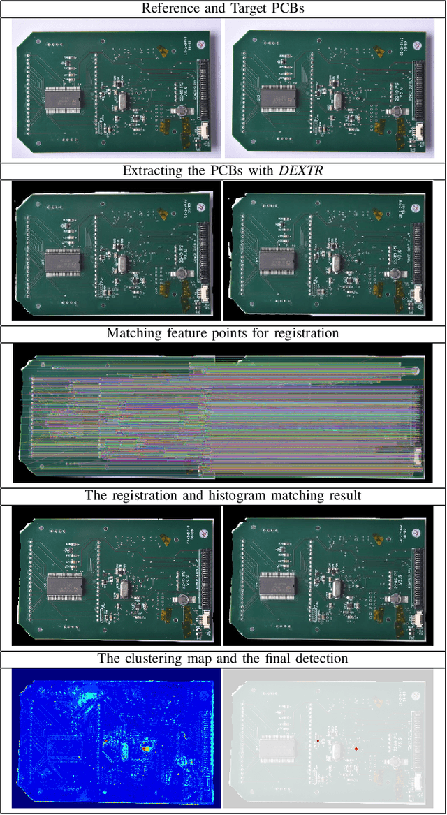
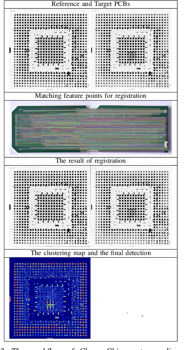

The usage of electronic devices increases, and becomes predominant in most aspects of life. Surface Mount Technology (SMT) is the most common industrial method for manufacturing electric devices in which electrical components are mounted directly onto the surface of a Printed Circuit Board (PCB). Although the expansion of electronic devices affects our lives in a productive way, failures or defects in the manufacturing procedure of those devices might also be counterproductive and even harmful in some cases. It is therefore desired and sometimes crucial to ensure zero-defect quality in electronic devices and their production. While traditional Image Processing (IP) techniques are not sufficient to produce a complete solution, other promising methods like Deep Learning (DL) might also be challenging for PCB inspection, mainly because such methods require big adequate datasets which are missing, not available or not updated in the rapidly growing field of PCBs. Thus, PCB inspection is conventionally performed manually by human experts. Unsupervised Learning (UL) methods may potentially be suitable for PCB inspection, having learning capabilities on the one hand, while not relying on large datasets on the other. In this paper, we introduce ChangeChip, an automated and integrated change detection system for defect detection in PCBs, from soldering defects to missing or misaligned electronic elements, based on Computer Vision (CV) and UL. We achieve good quality defect detection by applying an unsupervised change detection between images of a golden PCB (reference) and the inspected PCB under various setting. In this work, we also present CD-PCB, a synthesized labeled dataset of 20 pairs of PCB images for evaluation of defect detection algorithms.
Anomaly Detection for Solder Joints Using $β$-VAE
Apr 24, 2021
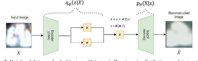
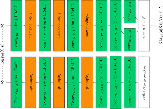
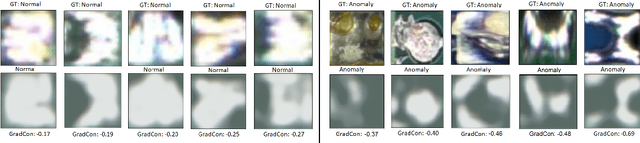
In the assembly process of printed circuit boards (PCB), most of the errors are caused by solder joints in Surface Mount Devices (SMD). In the literature, traditional feature extraction based methods require designing hand-crafted features and rely on the tiered RGB illumination to detect solder joint errors, whereas the supervised Convolutional Neural Network (CNN) based approaches require a lot of labelled abnormal samples (defective solder joints) to achieve high accuracy. To solve the optical inspection problem in unrestricted environments with no special lighting and without the existence of error-free reference boards, we propose a new beta-Variational Autoencoders (beta-VAE) architecture for anomaly detection that can work on both IC and non-IC components. We show that the proposed model learns disentangled representation of data, leading to more independent features and improved latent space representations. We compare the activation and gradient-based representations that are used to characterize anomalies; and observe the effect of different beta parameters on accuracy and on untwining the feature representations in beta-VAE. Finally, we show that anomalies on solder joints can be detected with high accuracy via a model trained on directly normal samples without designated hardware or feature engineering.
Deep Learning Based Defect Detection for Solder Joints on Industrial X-Ray Circuit Board Images
Aug 06, 2020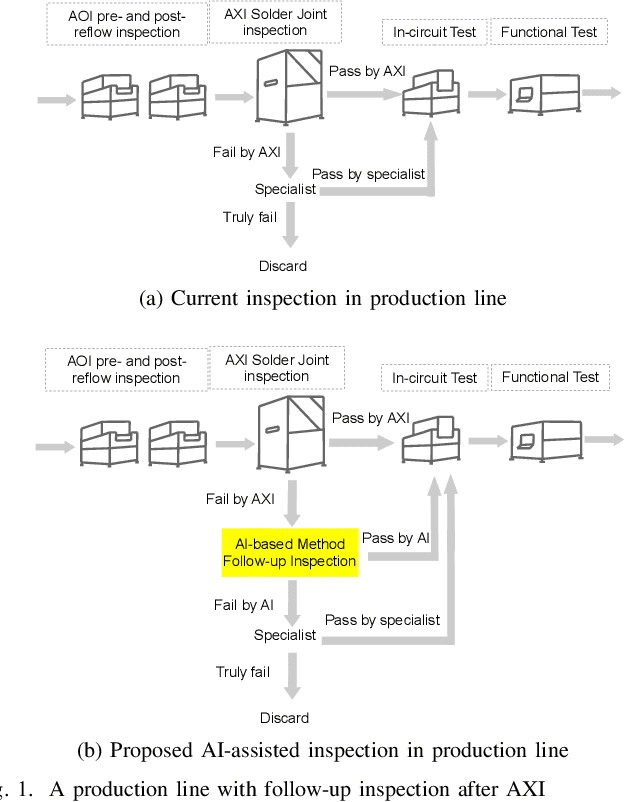
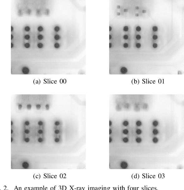
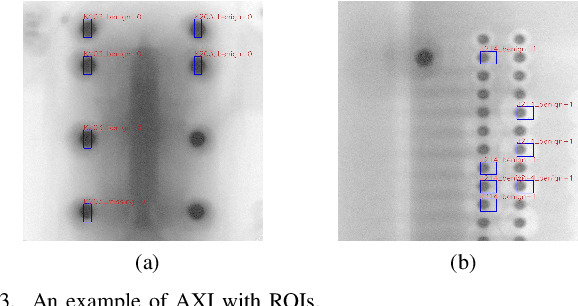
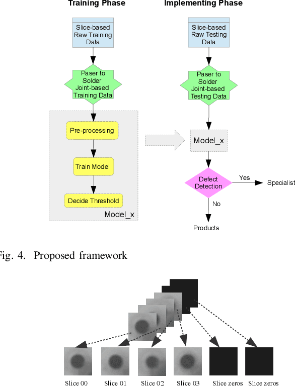
Quality control is of vital importance during electronics production. As the methods of producing electronic circuits improve, there is an increasing chance of solder defects during assembling the printed circuit board (PCB). Many technologies have been incorporated for inspecting failed soldering, such as X-ray imaging, optical imaging, and thermal imaging. With some advanced algorithms, the new technologies are expected to control the production quality based on the digital images. However, current algorithms sometimes are not accurate enough to meet the quality control. Specialists are needed to do a follow-up checking. For automated X-ray inspection, joint of interest on the X-ray image is located by region of interest (ROI) and inspected by some algorithms. Some incorrect ROIs deteriorate the inspection algorithm. The high dimension of X-ray images and the varying sizes of image dimensions also challenge the inspection algorithms. On the other hand, recent advances on deep learning shed light on image-based tasks and are competitive to human levels. In this paper, deep learning is incorporated in X-ray imaging based quality control during PCB quality inspection. Two artificial intelligence (AI) based models are proposed and compared for joint defect detection. The noised ROI problem and the varying sizes of imaging dimension problem are addressed. The efficacy of the proposed methods are verified through experimenting on a real-world 3D X-ray dataset. By incorporating the proposed methods, specialist inspection workload is largely saved.
Convolutional Recurrent Reconstructive Network for Spatiotemporal Anomaly Detection in Solder Paste Inspection
Aug 22, 2019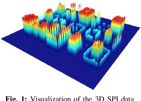
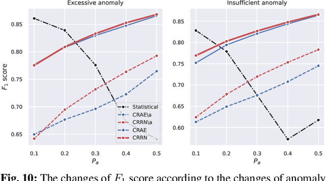
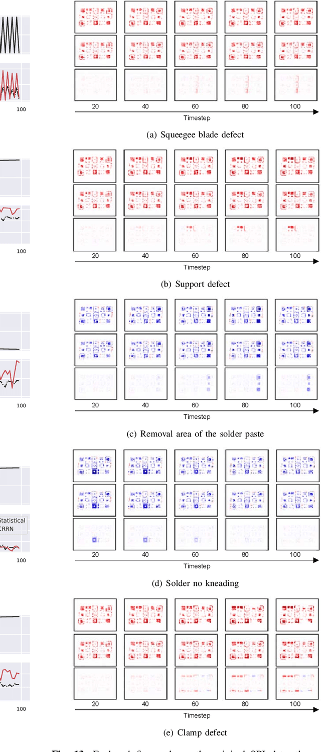
Surface mount technology (SMT) is a process for producing printed circuit boards. Solder paste printer (SPP), package mounter, and solder reflow oven are used for SMT. The board on which the solder paste is deposited from the SPP is monitored by solder paste inspector (SPI). If SPP malfunctions due to the printer defects, the SPP produces defective products, and then abnormal patterns are detected by SPI. In this paper, we propose a convolutional recurrent reconstructive network (CRRN), which decomposes the anomaly patterns generated by the printer defects, from SPI data. CRRN learns only normal data and detects anomaly pattern through reconstruction error. CRRN consists of a spatial encoder (S-Encoder), a spatiotemporal encoder and decoder (ST-Encoder-Decoder), and a spatial decoder (S-Decoder). The ST-Encoder-Decoder consists of multiple convolutional spatiotemporal memories (CSTMs) with ST-Attention mechanism. CSTM is developed to extract spatiotemporal patterns efficiently. Additionally, a spatiotemporal attention (ST-Attention) mechanism is designed to facilitate transmitting information from the ST-Encoder to the ST-Decoder, which can solve the long-term dependency problem. We demonstrate the proposed CRRN outperforms the other conventional models in anomaly detection. Moreover, we show the discriminative power of the anomaly map decomposed by the proposed CRRN through the printer defect classification.
Robust BGA Void Detection Using Multi Directional Scan Algorithms
Aug 31, 2019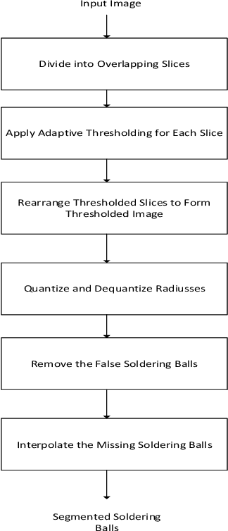
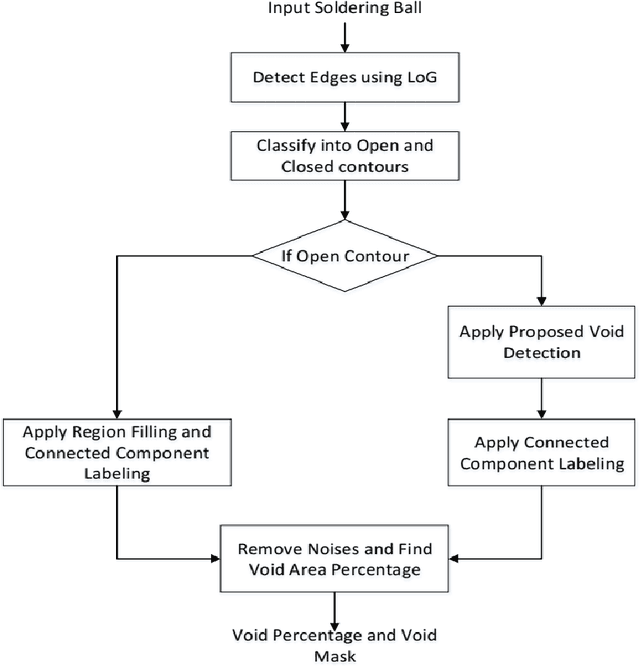
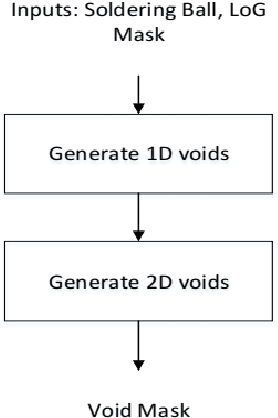
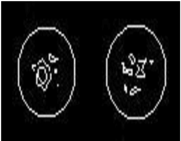
The life time of electronic circuits board are impacted by the voids present in soldering balls. The quality inspection of solder balls by detecting and measuring the void is important to improve the board yield issues in electronic circuits. In general, the inspection is carried out manually, based on 2D or 3D X-ray images. For high quality inspection, it is difficult to detect and measure voids accurately with high repeatability through the manual inspection and it is time consuming process. In need of high quality and fast inspection, various approaches were proposed for void detection. But, lacks in robustness in dealing with various challenges like vias, reflections from the plating or vias, inconsistent lighting, noise, void-like artefacts, various void shapes, low resolution images and scalability to various devices. Robust BGA void detection becomes quite difficult problem, especially if the image size is very small (say, around 40x40) and with low contrast between void and the BGA background (say around 7 intensity levels on a scale of 255). In this work, we propose novel approach for void detection based on the multi directional scanning. The proposed approach is able to segment the voids for low resolution images and can be easily scaled to various electronic manufacturing products.
Void region segmentation in ball grid array using u-net approach and synthetic data
Jul 07, 2019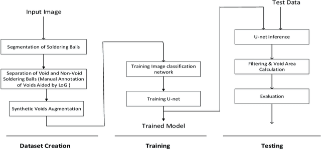
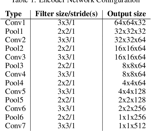
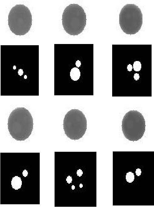
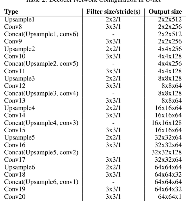
The quality inspection of solder balls by detecting and measuring the void is important to improve the board yield issues in electronic circuits. In general, the inspection is carried out manually, based on 2D or 3D X-ray images. For high quality inspection, it is difficult to detect and measure voids accurately with high repeatability through the manual inspection and the process is time consuming. In need of high quality and fast inspection, various approaches were proposed, but, due to the various challenges like vias, reflections from the plating or vias, inconsistent lighting, noise and void-like artifacts makes these approaches difficult to work in all these challenging conditions. In recent times, deep learning approaches are providing the outstanding accuracy in various computer vision tasks. Considering the need of high quality and fast inspection, in this paper, we applied U-Net to segment the void regions in soldering balls. As it is difficult to get the annotated dataset covering all the variations of void, we proposed an approach to generated the synthetic dataset. The proposed approach is able to segment the voids and can be easily scaled to various electronic products.