 Add to Chrome
 Add to Firefox
 Add to Edge
Fully Automatic In-Situ Reconfiguration of RF Photonic Filters in a CMOS-Compatible Silicon Photonic Process
May 23, 2022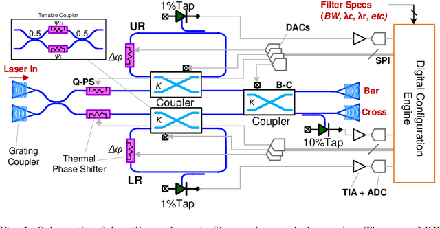
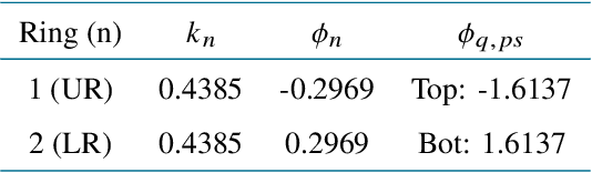
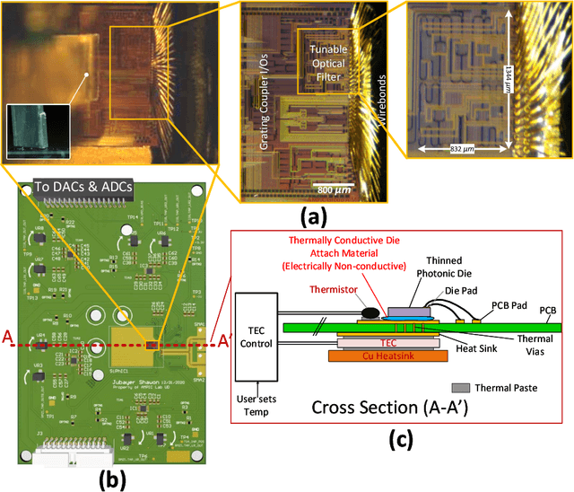
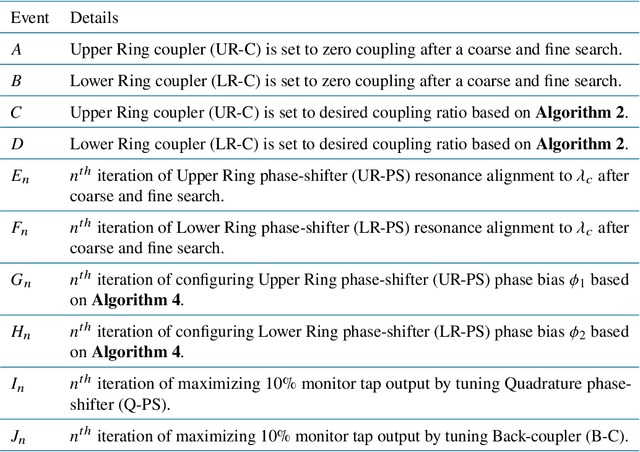
Automatic reconfiguration of optical filters is the key to novel flexible RF photonic receivers and Software Defined Radios (SDRs). Although silicon photonics (SiP) is a promising technology platform to realize such receivers, process variations and lack of in-situ tuning capability limits the adoption of SiP filters in widely-tunable RF photonic receivers. To address this issue, this work presents a first `in-situ' automatic reconfiguration algorithm and demonstrates a software configurable integrated optical filter that can be reconfigured on-the-fly based on user specifications. The presented reconfiguration scheme avoids the use of expensive and bulky equipment such as Optical Vector Network Analyzer (OVNA), does not use simulation data for reconfiguration, reduces the total number of thermo-optic tuning elements required and eliminates several time consuming configuration steps as in the prior art. This makes this filter ideal in a real world scenario where user specifies the filter center frequency, bandwidth, required rejection & filter type (Butterworth, Chebyshev, etc.) and the filter is automatically configured regardless of process, voltage & temperature (PVT) variations. We fabricated our design in AIM Photonics' Active SiP process and have demonstrated our reconfiguration algorithm for a second-order filter with 3dB bandwidth of 3 GHz, 2.2 dB insertion loss and >30 dB out-of-band rejection using only two reference laser wavelength settings. Since the filter photonic integrated circuit (PIC) is fabricated using a CMOS-compatible SiP foundry, the design is manufacturable with repeatable and scalable performance suited for its integration with electronics to realize complex chip-scale RF photonic systems.
Analysis of Trade-offs in RF Photonic Links based on Multi-Bias Tuning of Silicon Photonic Ring-Assisted Mach Zehnder Modulators
Sep 27, 2021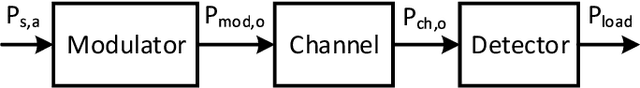
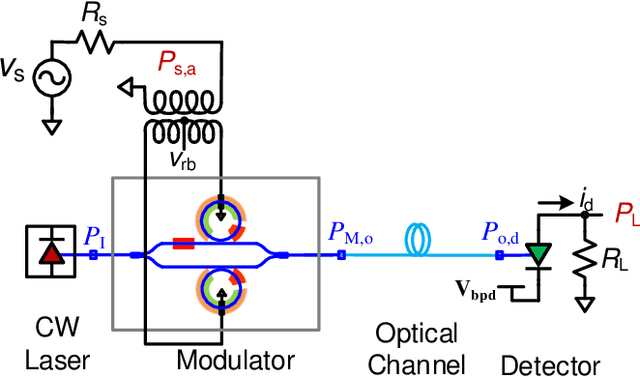
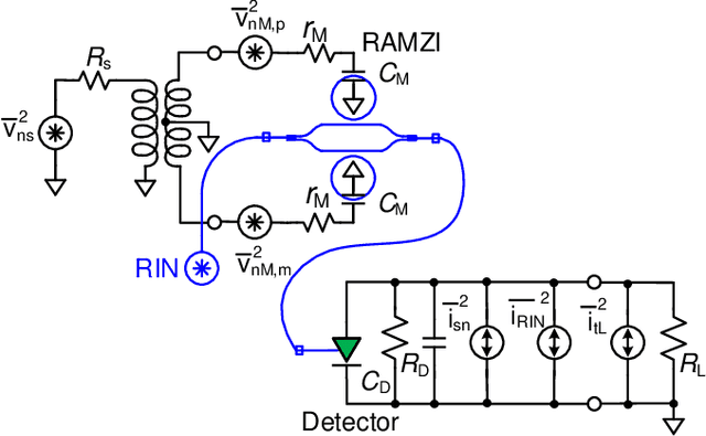
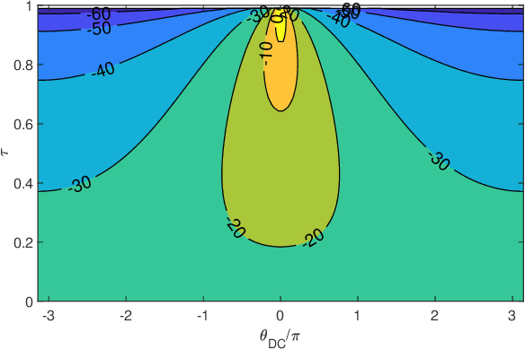
Recent progress in silicon-based photonic integrated circuits (PICs) have opened new avenues for analog circuit designers to explore hybrid integration of photonics with CMOS ICs. Traditionally, optoelectronic systems are designed using discrete optics and electronics. Silicon photonic (SiP) platforms provide the opportunity to realize these systems in a compact chip-scale form factor and alleviate long-standing challenges in optoelectronics. In this work, we analyze multi-bias tuning in Ring-Assisted Mach Zehnder Modulator (RAMZM) and resulting trade-offs in analog RF photonic links realized using RAMZMs. Multi-bias tuning in the rings and the Mach-Zehnder arms allow informed trade-offs between link noise figure and linearity. We derive performance metrics including gain, noise figure, and linearity metrics associated with tuning of multiple bias settings in RAMZM based links and present resulting design optimization. Compared to MZM, an improvement of 18 dB/Hz$^{\frac{2}{3}}$ in SFDR is noted when RAMZM is linearized. We also propose a biasing scheme for RAMZM that provides 6x improvement in slope efficiency, or equivalently, 15.56dB in power Gain over MZMs (single drive) while still providing similar SFDR performance ($\sim$ 109 dB/Hz$^{\frac{2}{3}}$) as MZMs. Moreover, a method to improve gain in photodiode saturation limited links is presented and studied.
Continuous Learning in a Single-Incremental-Task Scenario with Spike Features
May 03, 2020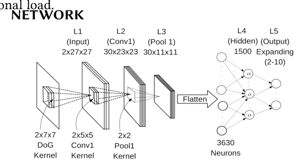
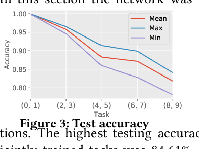
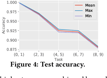
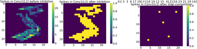
Deep Neural Networks (DNNs) have two key deficiencies, their dependence on high precision computing and their inability to perform sequential learning, that is, when a DNN is trained on a first task and the same DNN is trained on the next task it forgets the first task. This phenomenon of forgetting previous tasks is also referred to as catastrophic forgetting. On the other hand a mammalian brain outperforms DNNs in terms of energy efficiency and the ability to learn sequentially without catastrophically forgetting. Here, we use bio-inspired Spike Timing Dependent Plasticity (STDP)in the feature extraction layers of the network with instantaneous neurons to extract meaningful features. In the classification sections of the network we use a modified synaptic intelligence that we refer to as cost per synapse metric as a regularizer to immunize the network against catastrophic forgetting in a Single-Incremental-Task scenario (SIT). In this study, we use MNIST handwritten digits dataset that was divided into five sub-tasks.
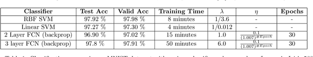
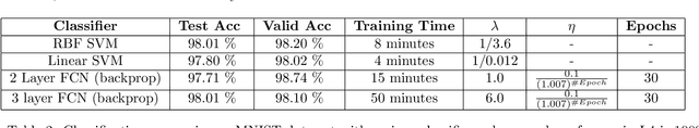
A Deep Unsupervised Feature Learning Spiking Neural Network with Binarized Classification Layers for EMNIST Classification
Feb 26, 2020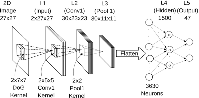
End user AI is trained on large server farms with data collected from the users. With ever increasing demand for IOT devices, there is a need for deep learning approaches that can be implemented (at the edge) in an energy efficient manner. In this work we approach this using spiking neural networks. The unsupervised learning technique of spike timing dependent plasticity (STDP) using binary activations are used to extract features from spiking input data. Gradient descent (backpropagation) is used only on the output layer to perform the training for classification. The accuracies obtained for the balanced EMNIST data set compare favorably with other approaches. The effect of stochastic gradient descent (SGD) approximations on learning capabilities of our network are also explored.
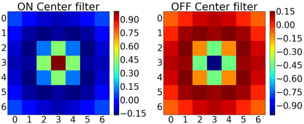
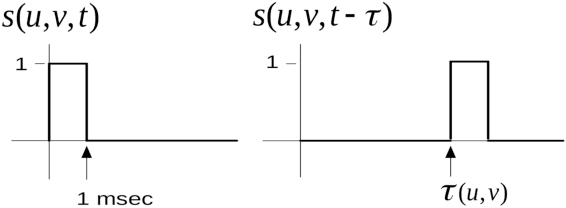
Deep Convolutional Spiking Neural Networks for Image Classification
Mar 28, 2019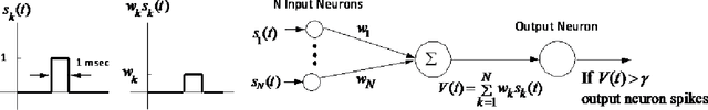
Spiking neural networks are biologically plausible counterparts of the artificial neural networks, artificial neural networks are usually trained with stochastic gradient descent and spiking neural networks are trained with spike timing dependant plasticity. Training deep convolutional neural networks is a memory and power intensive job. Spiking networks could potentially help in reducing the power usage. There is a large pool of tools for one to chose to train artificial neural networks of any size, on the other hand all the available tools to simulate spiking neural networks are geared towards computational neuroscience applications and they are not suitable for real life applications. In this work we focus on implementing a spiking CNN using Tensorflow to examine behaviour of the network and empirically study the effect of various parameters on learning capabilities and also study catastrophic forgetting in the spiking CNN and weight initialization problem in R-STDP using MNIST and N-MNIST data sets.
Energy-Efficient CMOS Memristive Synapses for Mixed-Signal Neuromorphic System-on-a-Chip
Apr 20, 2018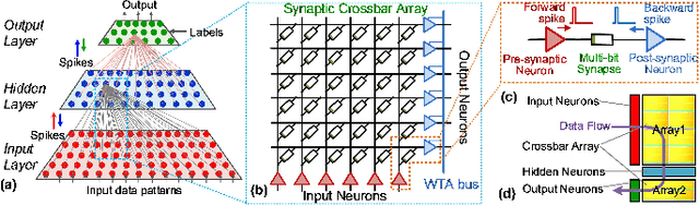
Emerging non-volatile memory (NVM), or memristive, devices promise energy-efficient realization of deep learning, when efficiently integrated with mixed-signal integrated circuits on a CMOS substrate. Even though several algorithmic challenges need to be addressed to turn the vision of memristive Neuromorphic Systems-on-a-Chip (NeuSoCs) into reality, issues at the device and circuit interface need immediate attention from the community. In this work, we perform energy-estimation of a NeuSoC system and predict the desirable circuit and device parameters for energy-efficiency optimization. Also, CMOS synapse circuits based on the concept of CMOS memristor emulator are presented as a system prototyping methodology, while practical memristor devices are being developed and integrated with general-purpose CMOS. The proposed mixed-signal memristive synapse can be designed and fabricated using standard CMOS technologies and open doors to interesting applications in cognitive computing circuits.
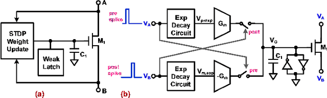
Dendritic-Inspired Processing Enables Bio-Plausible STDP in Compound Binary Synapses
Jan 09, 2018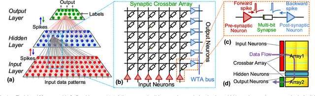
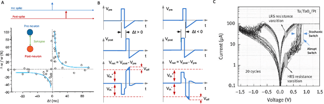
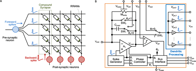
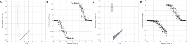
Brain-inspired learning mechanisms, e.g. spike timing dependent plasticity (STDP), enable agile and fast on-the-fly adaptation capability in a spiking neural network. When incorporating emerging nanoscale resistive non-volatile memory (NVM) devices, with ultra-low power consumption and high-density integration capability, a spiking neural network hardware would result in several orders of magnitude reduction in energy consumption at a very small form factor and potentially herald autonomous learning machines. However, actual memory devices have shown to be intrinsically binary with stochastic switching, and thus impede the realization of ideal STDP with continuous analog values. In this work, a dendritic-inspired processing architecture is proposed in addition to novel CMOS neuron circuits. The utilization of spike attenuations and delays transforms the traditionally undesired stochastic behavior of binary NVMs into a useful leverage that enables biologically-plausible STDP learning. As a result, this work paves a pathway to adopt practical binary emerging NVM devices in brain-inspired neuromorphic computing.
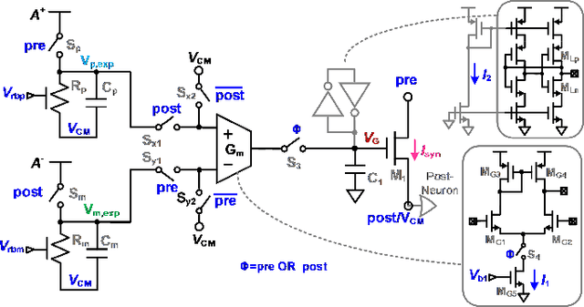
Enabling Bio-Plausible Multi-level STDP using CMOS Neurons with Dendrites and Bistable RRAMs
Dec 19, 2016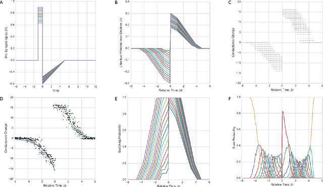
Large-scale integration of emerging nanoscale non-volatile memory devices, e.g. resistive random-access memory (RRAM), can enable a new generation of neuromorphic computers that can solve a wide range of machine learning problems. Such hybrid CMOS-RRAM neuromorphic architectures will result in several orders of magnitude reduction in energy consumption at a very small form factor, and herald autonomous learning machines capable of self-adapting to their environment. However, the progress in this area has been impeded from the realization that the actual memory devices fall well short of their expected behavior. In this work, we discuss the challenges associated with these memory devices and their use in neuromorphic computing circuits, and propose pathways to overcome these limitations by introducing 'dendritic learning'.
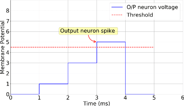
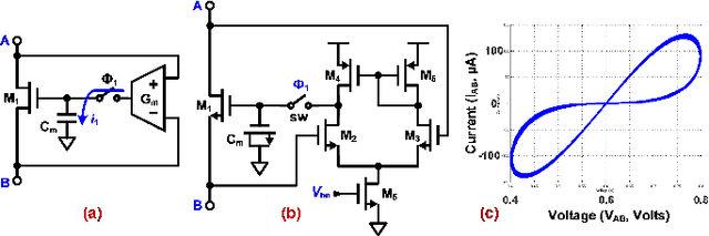
A CMOS Spiking Neuron for Brain-Inspired Neural Networks with Resistive Synapses and In-Situ Learning
Nov 24, 2015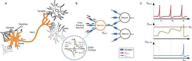
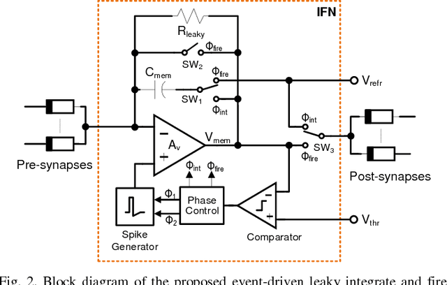
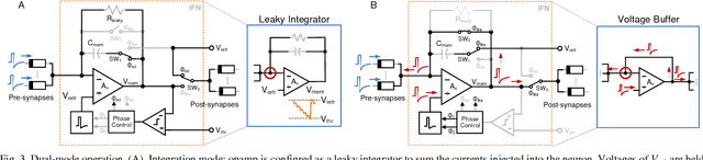
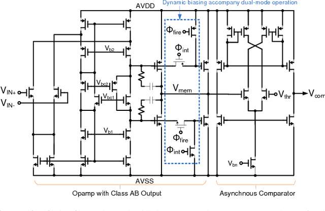
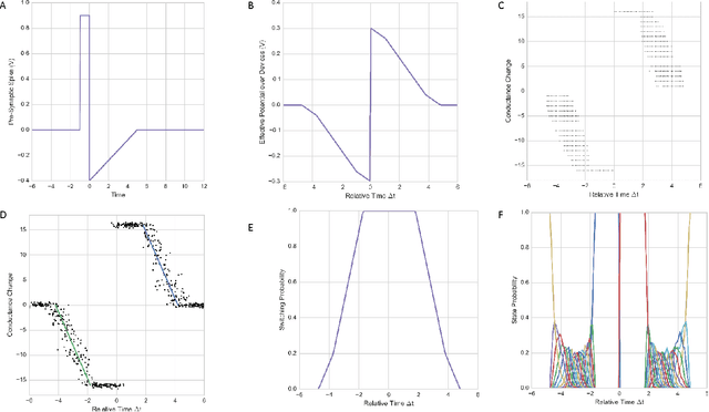
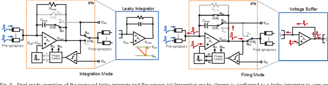
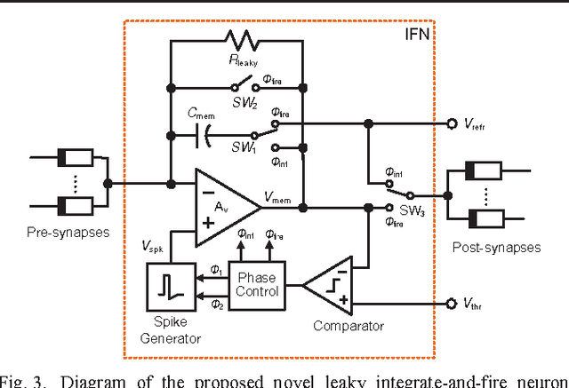
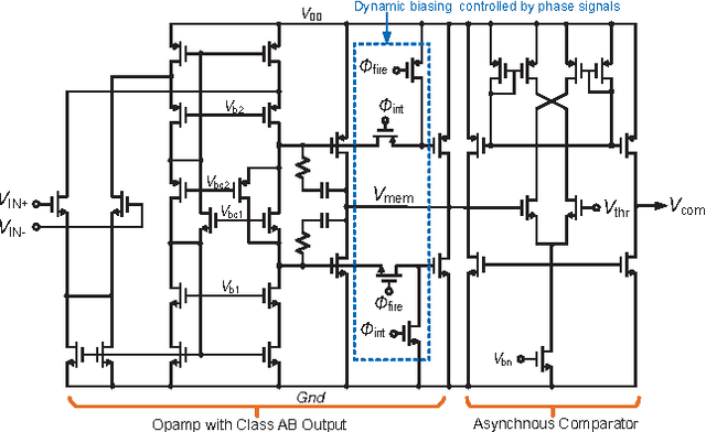
Nanoscale resistive memories are expected to fuel dense integration of electronic synapses for large-scale neuromorphic system. To realize such a brain-inspired computing chip, a compact CMOS spiking neuron that performs in-situ learning and computing while driving a large number of resistive synapses is desired. This work presents a novel leaky integrate-and-fire neuron design which implements the dual-mode operation of current integration and synaptic drive, with a single opamp and enables in-situ learning with crossbar resistive synapses. The proposed design was implemented in a 0.18 $\mu$m CMOS technology. Measurements show neuron's ability to drive a thousand resistive synapses, and demonstrate an in-situ associative learning. The neuron circuit occupies a small area of 0.01 mm$^2$ and has an energy-efficiency of 9.3 pJ$/$spike$/$synapse.
A CMOS Spiking Neuron for Dense Memristor-Synapse Connectivity for Brain-Inspired Computing
Jun 08, 2015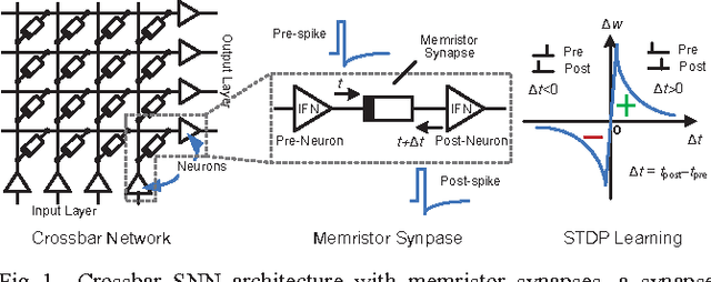
Neuromorphic systems that densely integrate CMOS spiking neurons and nano-scale memristor synapses open a new avenue of brain-inspired computing. Existing silicon neurons have molded neural biophysical dynamics but are incompatible with memristor synapses, or used extra training circuitry thus eliminating much of the density advantages gained by using memristors, or were energy inefficient. Here we describe a novel CMOS spiking leaky integrate-and-fire neuron circuit. Building on a reconfigurable architecture with a single opamp, the described neuron accommodates a large number of memristor synapses, and enables online spike timing dependent plasticity (STDP) learning with optimized power consumption. Simulation results of an 180nm CMOS design showed 97% power efficiency metric when realizing STDP learning in 10,000 memristor synapses with a nominal 1M{\Omega} memristance, and only 13{\mu}A current consumption when integrating input spikes. Therefore, the described CMOS neuron contributes a generalized building block for large-scale brain-inspired neuromorphic systems.