 Add to Chrome
 Add to Firefox
 Add to Edge
ADVERSARIAL: And-Inverter Graph-Assisted Hardware Trojan Detection At Scale
Jul 26, 2026
Modern System-on-Chip (SoCs) often contain hundreds of millions to tens of billions of gates, making existing Hardware Trojan (HT) detection methods impractical due to their immense scale. The proposed approach incorporates symbolically enabled learning by modeling flattened gate-level netlists as Boolean networks represented as And-Inverter Graphs (AIGs), where all internal nodes are 2-input AND gates and inversions reside on the edges. Each directed connection is expressed as a triple within a Knowledge Graph Embedding (KGE) framework, producing compact, constant-size per-node representations that retain multi-hop structural context. The AIG's bounded fan-in and uniform semantics ensure training and inference complexity scale linearly with edge count, addressing major scalability bottlenecks in HT detection. Symbolically enabled learning across deep datapaths enables the model to differentiate circuit structures from rare and functionally inconsistent connections that signify potential Trojan triggers and payloads. Experiments on large-scale SoC benchmarks demonstrate clear geometric separation between Trojan and benign nodes and practical scalability.

A Comprehensive Design Framework for Vertical Power Delivery in High-Performance Computing
Jun 27, 2026Power delivery -- including high-to-low voltage conversion, complex power distribution across heterogeneously integrated chiplets, and efficient interconnect allocation -- remains a critical bottleneck in high-performance computing (HPC) systems. Existing vertical power delivery (VPD) solutions are estimated to achieve less than 70\% system-wide end-to-end power delivery efficiency, defined from platform input power to delivered on-chip load power, with substantial energy lost as heat before reaching on-chip point-of-loads (POLs). In the absence of systematic design methodologies, evaluating power quality, exploring architectural alternatives, and optimizing performance rely on computationally prohibitive simulations, resulting in suboptimal designs. This paper introduces an end-to-end scalable power delivery framework for HPC systems, including distributed VPD (DVPD) architecture, DVPD design optimization methodology, and analytical models. The framework leverages substrate-embedded GaN power switches together with arrays of unit inductors and capacitors tailored for HPC applications. Multi-stage power conversion schemes (48V-to-1V, 48V-to-24V-to-1V, and 48V-to-12V-to-1V) are explored, with system-wide voltage drops and power losses evaluated under steady-state conditions. Design specifications for passive and active devices are formulated to meet next-generation efficiency targets. For the 48V-to-1V case, the proposed DVPD approach achieves 84\% system-wide efficiency while occupying 54\% of the area beneath the load system, with efficiency increasing to 87.6\% at 75\% area utilization across a 1--50~kW load range. Furthermore, steady-state voltage drops peak at 2.7\% and transient drops at 9\% (without decoupling capacitors), demonstrating the viability of DVPD for future wafer-scale HPC platforms.
PALTO: Physics-Informed Active Learning for Tri-Gate FinFET Design Optimization for Vertical Power Delivery
May 31, 2026This paper demonstrates the effectiveness of machine learning-driven optimization for designing application-specific GaN tri-gate FinFETs in vertical power delivery systems. Conventional TCAD-based approaches are computationally intensive and insufficient for navigating the high-dimensional, nonlinear design space of advanced GaN devices. To address this, a physics-informed active learning framework is used to intelligently guide simulations, accelerating convergence while preserving accuracy. This ML-guided approach enables the discovery of optimal configurations by efficiently exploring key structural parameters -- most notably the GaN-to-AlGaN thickness ratio -- a long-standing focus of debate in device design. By systematically exploring key structural parameters, two optimized devices with aggressively scaled gate-to-drain lengths are identified. Single-fin, multi-channel simulations show that device~D2, with a thinner GaN channel relative to the AlGaN barrier, achieves higher drive current. However, in a 300-fin configuration, device~D1 outperforms device~D2 by delivering 3.3\,A at 0.49~ohm on-resistance -- approximately 2$\times$ better -- despite slightly higher parasitics. Both devices operate in a normally-off mode. Based on an application-specific figure of merit, device~D1 achieves 5\,pC$\cdot$ohm, demonstrating 2$\times$ greater switching efficiency than device~D2, while both designs outperform industrial benchmarks from different performance standpoints.
From Physics to Surrogate Intelligence: A Unified Electro-Thermo-Optimization Framework for TSV Networks
Mar 31, 2026High-density through-substrate vias (TSVs) enable 2.5D/3D heterogeneous integration but introduce significant signal-integrity and thermal-reliability challenges due to electrical coupling, insertion loss, and self-heating. Conventional full-wave finite-element method (FEM) simulations provide high accuracy but become computationally prohibitive for large design-space exploration. This work presents a scalable electro-thermal modeling and optimization framework that combines physics-informed analytical modeling, graph neural network (GNN) surrogates, and full-wave sign-off validation. A multi-conductor analytical model computes broadband S-parameters and effective anisotropic thermal conductivities of TSV arrays, achieving $5\%-10\%$ relative Frobenius error (RFE) across array sizes up to $15x15$. A physics-informed GNN surrogate (TSV-PhGNN), trained on analytical data and fine-tuned with HFSS simulations, generalizes to larger arrays with RFE below $2\%$ and nearly constant variance. The surrogate is integrated into a multi-objective Pareto optimization framework targeting reflection coefficient, insertion loss, worst-case crosstalk (NEXT/FEXT), and effective thermal conductivity. Millions of TSV configurations can be explored within minutes, enabling exhaustive layout and geometric optimization that would be infeasible using FEM alone. Final designs are validated with Ansys HFSS and Mechanical, showing strong agreement. The proposed framework enables rapid electro-thermal co-design of TSV arrays while reducing per-design evaluation time by more than six orders of magnitude.
Automated Hardware Trojan Insertion in Industrial-Scale Designs
Nov 11, 2025Industrial Systems-on-Chips (SoCs) often comprise hundreds of thousands to millions of nets and millions to tens of millions of connectivity edges, making empirical evaluation of hardware-Trojan (HT) detectors on realistic designs both necessary and difficult. Public benchmarks remain significantly smaller and hand-crafted, while releasing truly malicious RTL raises ethical and operational risks. This work presents an automated and scalable methodology for generating HT-like patterns in industry-scale netlists whose purpose is to stress-test detection tools without altering user-visible functionality. The pipeline (i) parses large gate-level designs into connectivity graphs, (ii) explores rare regions using SCOAP testability metrics, and (iii) applies parameterized, function-preserving graph transformations to synthesize trigger-payload pairs that mimic the statistical footprint of stealthy HTs. When evaluated on the benchmarks generated in this work, representative state-of-the-art graph-learning models fail to detect Trojans. The framework closes the evaluation gap between academic circuits and modern SoCs by providing reproducible challenge instances that advance security research without sharing step-by-step attack instructions.
A Unified Learning Platform for Dynamic Frequency Scaling in Pipelined Processors
Jun 12, 2020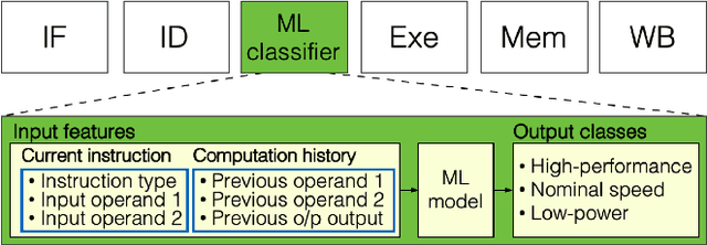
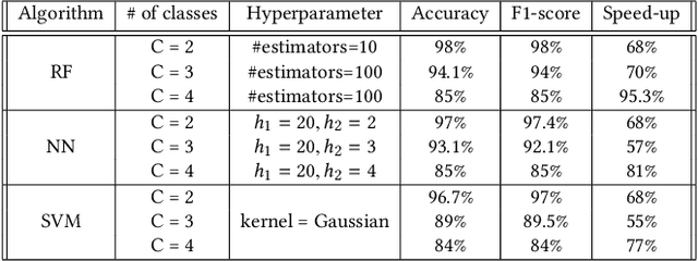
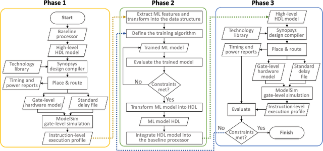
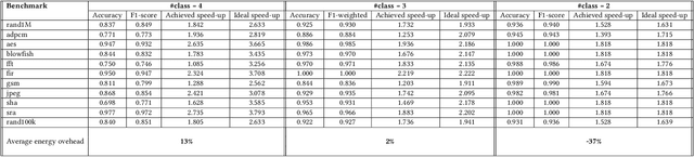
A machine learning (ML) design framework is proposed for dynamically adjusting clock frequency based on propagation delay of individual instructions. A Random Forest model is trained to classify propagation delays in real-time, utilizing current operation type, current operands, and computation history as ML features. The trained model is implemented in Verilog as an additional pipeline stage within a baseline processor. The modified system is simulated at the gate-level in 45 nm CMOS technology, exhibiting a speed-up of 68% and energy reduction of 37% with coarse-grained ML classification. A speed-up of 95% is demonstrated with finer granularities at additional energy costs.
Progressive VAE Training on Highly Sparse and Imbalanced Data
Dec 17, 2019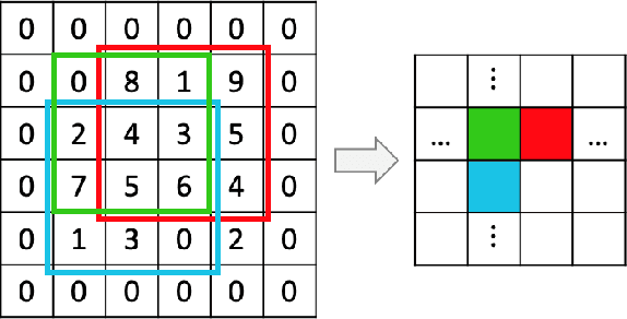
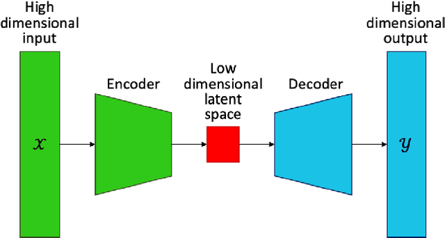
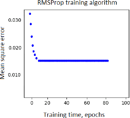
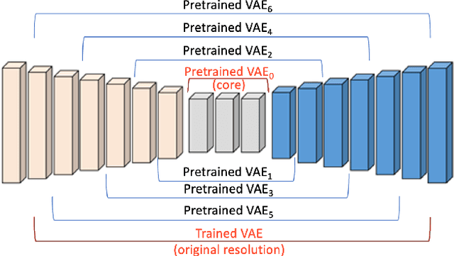
In this paper, we present a novel approach for training a Variational Autoencoder (VAE) on a highly imbalanced data set. The proposed training of a high-resolution VAE model begins with the training of a low-resolution core model, which can be successfully trained on imbalanced data set. In subsequent training steps, new convolutional, upsampling, deconvolutional, and downsampling layers are iteratively attached to the model. In each iteration, the additional layers are trained based on the intermediate pretrained model - a result of previous training iterations. Thus, the resolution of the model is progressively increased up to the required resolution level. In this paper, the progressive VAE training is exploited for learning a latent representation with imbalanced, highly sparse data sets and, consequently, generating routes in a constrained 2D space. Routing problems (e.g., vehicle routing problem, travelling salesman problem, and arc routing) are of special significance in many modern applications (e.g., route planning, network maintenance, developing high-performance nanoelectronic systems, and others) and typically associated with sparse imbalanced data. In this paper, the critical problem of routing billions of components in nanoelectronic devices is considered. The proposed approach exhibits a significant training speedup as compared with state-of-the-art existing VAE training methods, while generating expected image outputs from unseen input data. Furthermore, the final progressive VAE models exhibit much more precise output representation, than the Generative Adversarial Network (GAN) models trained with comparable training time. The proposed method is expected to be applicable to a wide range of applications, including but not limited image impainting, sentence interpolation, and semi-supervised learning.
Exploiting Dual-Gate Ambipolar CNFETs for Scalable Machine Learning Classification
Dec 09, 2019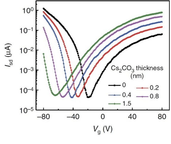
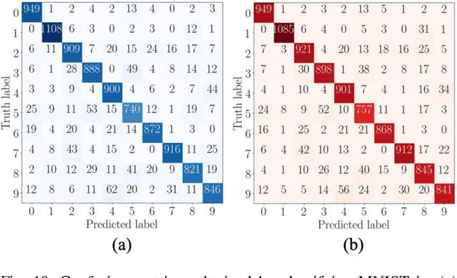
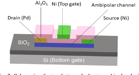
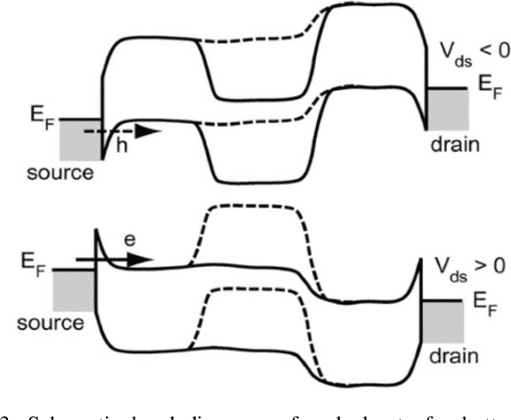
Ambipolar carbon nanotube based field-effect transistors (AP-CNFETs) exhibit unique electrical characteristics, such as tri-state operation and bi-directionality, enabling systems with complex and reconfigurable computing. In this paper, AP-CNFETs are used to design a mixed-signal machine learning (ML) classifier. The classifier is designed in SPICE with feature size of 15 nm and operates at 250 MHz. The system is demonstrated based on MNIST digit dataset, yielding 90% accuracy and no accuracy degradation as compared with the classification of this dataset in Python. The system also exhibits lower power consumption and smaller physical size as compared with the state-of-the-art CMOS and memristor based mixed-signal classifiers.
A Single-MOSFET MAC for Confidence and Resolution Driven Machine Learning Classification
Oct 21, 2019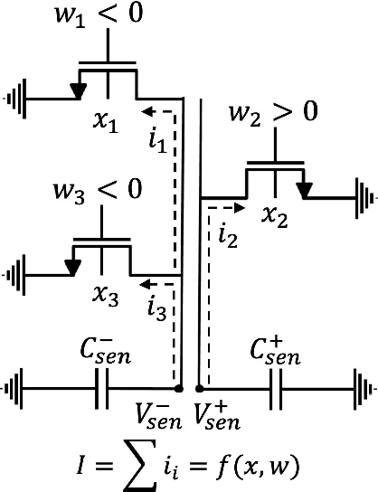
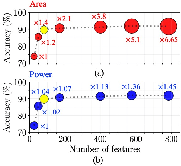
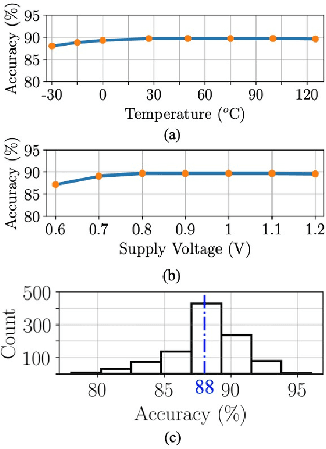
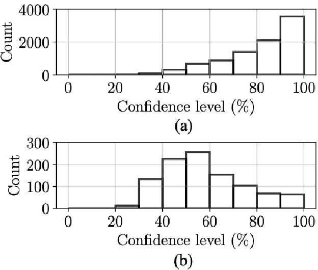
Mixed-signal machine-learning classification has recently been demonstrated as an efficient alternative for classification with power expensive digital circuits. In this paper, a high-COnfidence high-REsolution (CORE) mixed-signal classifier is proposed for classifying high-dimensional input data into multi-class output space with less power and area than state-of-the-art classifiers. A high-resolution multiplication is facilitated within a single-MOSFET by feeding the features and feature weights into, respectively, the body and gate inputs. High-resolution classifier that considers the confidence of the individual predictors is designed at 45 nm technology node and operates at 100 MHz in subthreshold region. To evaluate the performance of the classifier, a reduced MNIST dataset is generated by downsampling the MNIST digit images from 28 $\times$ 28 features to 9 $\times$ 9 features. The system is simulated across a wide range of PVT variations, exhibiting nominal accuracy of 90%, energy consumption of 6.2 pJ per classification (over 45 times lower than state-of-the-art classifiers), area of 2,179 $\mu$$m^{2}$ (over 7.3 times lower than state-of-the-art classifiers), and a stable response under PVT variations.