 Add to Chrome
 Add to Firefox
 Add to Edge
Wafer Defect Pattern Recognition
Papers and Code
Efficient Mixed-Type Wafer Defect Pattern Recognition Using Compact Deformable Convolutional Transformers
Mar 24, 2023


Manufacturing wafers is an intricate task involving thousands of steps. Defect Pattern Recognition (DPR) of wafer maps is crucial to find the root cause of the issue and further improving the yield in the wafer foundry. Mixed-type DPR is much more complicated compared to single-type DPR due to varied spatial features, the uncertainty of defects, and the number of defects present. To accurately predict the number of defects as well as the types of defects, we propose a novel compact deformable convolutional transformer (DC Transformer). Specifically, DC Transformer focuses on the global features present in the wafer map by virtue of learnable deformable kernels and multi-head attention to the global features. The proposed method succinctly models the internal relationship between the wafer maps and the defects. DC Transformer is evaluated on a real dataset containing 38 defect patterns. Experimental results show that DC Transformer performs exceptionally well in recognizing both single and mixed-type defects. The proposed method outperforms the current state of the models by a considerable margin
An Embarrassingly Simple Approach for Wafer Feature Extraction and Defect Pattern Recognition
Mar 21, 2023Identifying defect patterns in a wafer map during manufacturing is crucial to find the root cause of the underlying issue and provides valuable insights on improving yield in the foundry. Currently used methods use deep neural networks to identify the defects. These methods are generally very huge and have significant inference time. They also require GPU support to efficiently operate. All these issues make these models not fit for on-line prediction in the manufacturing foundry. In this paper, we propose an extremely simple yet effective technique to extract features from wafer images. The proposed method is extremely fast, intuitive, and non-parametric while being explainable. The experiment results show that the proposed pipeline outperforms conventional deep learning models. Our feature extraction requires no training or fine-tuning while preserving the relative shape and location of data points as revealed by our interpretability analysis.
Mixed-Type Wafer Classification For Low Memory Devices Using Knowledge Distillation
Mar 24, 2023


Manufacturing wafers is an intricate task involving thousands of steps. Defect Pattern Recognition (DPR) of wafer maps is crucial for determining the root cause of production defects, which may further provide insight for yield improvement in wafer foundry. During manufacturing, various defects may appear standalone in the wafer or may appear as different combinations. Identifying multiple defects in a wafer is generally harder compared to identifying a single defect. Recently, deep learning methods have gained significant traction in mixed-type DPR. However, the complexity of defects requires complex and large models making them very difficult to operate on low-memory embedded devices typically used in fabrication labs. Another common issue is the unavailability of labeled data to train complex networks. In this work, we propose an unsupervised training routine to distill the knowledge of complex pre-trained models to lightweight deployment-ready models. We empirically show that this type of training compresses the model without sacrificing accuracy despite being up to 10 times smaller than the teacher model. The compressed model also manages to outperform contemporary state-of-the-art models.
Deep Open-Set Recognition for Silicon Wafer Production Monitoring
Aug 30, 2022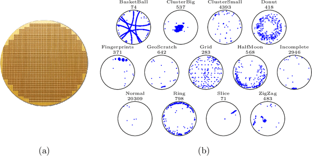
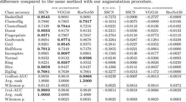
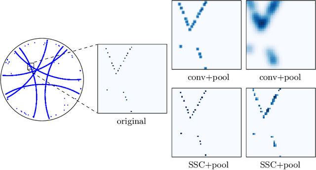
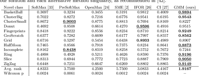
The chips contained in any electronic device are manufactured over circular silicon wafers, which are monitored by inspection machines at different production stages. Inspection machines detect and locate any defect within the wafer and return a Wafer Defect Map (WDM), i.e., a list of the coordinates where defects lie, which can be considered a huge, sparse, and binary image. In normal conditions, wafers exhibit a small number of randomly distributed defects, while defects grouped in specific patterns might indicate known or novel categories of failures in the production line. Needless to say, a primary concern of semiconductor industries is to identify these patterns and intervene as soon as possible to restore normal production conditions. Here we address WDM monitoring as an open-set recognition problem to accurately classify WDM in known categories and promptly detect novel patterns. In particular, we propose a comprehensive pipeline for wafer monitoring based on a Submanifold Sparse Convolutional Network, a deep architecture designed to process sparse data at an arbitrary resolution, which is trained on the known classes. To detect novelties, we define an outlier detector based on a Gaussian Mixture Model fitted on the latent representation of the classifier. Our experiments on a real dataset of WDMs show that directly processing full-resolution WDMs by Submanifold Sparse Convolutions yields superior classification performance on known classes than traditional Convolutional Neural Networks, which require a preliminary binning to reduce the size of the binary images representing WDMs. Moreover, our solution outperforms state-of-the-art open-set recognition solutions in detecting novelties.
Improving Automated Visual Fault Detection by Combining a Biologically Plausible Model of Visual Attention with Deep Learning
Feb 13, 2021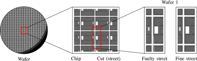
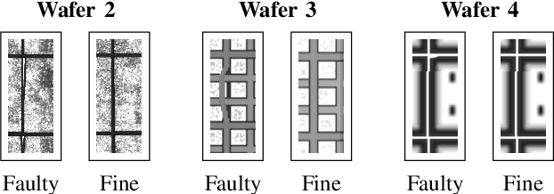
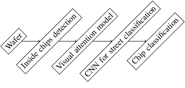
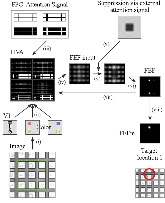
It is a long-term goal to transfer biological processing principles as well as the power of human recognition into machine vision and engineering systems. One of such principles is visual attention, a smart human concept which focuses processing on a part of a scene. In this contribution, we utilize attention to improve the automatic detection of defect patterns for wafers within the domain of semiconductor manufacturing. Previous works in the domain have often utilized classical machine learning approaches such as KNNs, SVMs, or MLPs, while a few have already used modern approaches like deep neural networks (DNNs). However, one problem in the domain is that the faults are often very small and have to be detected within a larger size of the chip or even the wafer. Therefore, small structures in the size of pixels have to be detected in a vast amount of image data. One interesting principle of the human brain for solving this problem is visual attention. Hence, we employ here a biologically plausible model of visual attention for automatic visual inspection. We propose a hybrid system of visual attention and a deep neural network. As demonstrated, our system achieves among other decisive advantages an improvement in accuracy from 81% to 92%, and an increase in accuracy for detecting faults from 67% to 88%. Hence, the error rates are reduced from 19% to 8%, and notably from 33% to 12% for detecting a fault in a chip. These results show that attention can greatly improve the performance of visual inspection systems. Furthermore, we conduct a broad evaluation, identifying specific advantages of the biological attention model in this application, and benchmarks standard deep learning approaches as an alternative with and without attention. This work is an extended arXiv version of the original conference article published in "IECON 2020", which has been extended regarding visual attention.