 Add to Chrome
 Add to Firefox
 Add to Edge
A Retina-Inspired Pathway to Real-Time Motion Prediction inside Image Sensors for Extreme-Edge Intelligence
Apr 02, 2025The ability to predict motion in real time is fundamental to many maneuvering activities in animals, particularly those critical for survival, such as attack and escape responses. Given its significance, it is no surprise that motion prediction in animals begins in the retina. Similarly, autonomous systems utilizing computer vision could greatly benefit from the capability to predict motion in real time. Therefore, for computer vision applications, motion prediction should be integrated directly at the camera pixel level. Towards that end, we present a retina-inspired neuromorphic framework capable of performing real-time, energy-efficient MP directly within camera pixels. Our hardware-algorithm framework, implemented using GlobalFoundries 22nm FDSOI technology, integrates key retinal MP compute blocks, including a biphasic filter, spike adder, nonlinear circuit, and a 2D array for multi-directional motion prediction. Additionally, integrating the sensor and MP compute die using a 3D Cu-Cu hybrid bonding approach improves design compactness by minimizing area usage and simplifying routing complexity. Validated on real-world object stimuli, the model delivers efficient, low-latency MP for decision-making scenarios reliant on predictive visual computation, while consuming only 18.56 pJ/MP in our mixed-signal hardware implementation.
Voltage-Controlled Magnetic Tunnel Junction based ADC-less Global Shutter Processing-in-Pixel for Extreme-Edge Intelligence
Oct 14, 2024


The vast amount of data generated by camera sensors has prompted the exploration of energy-efficient processing solutions for deploying computer vision tasks on edge devices. Among the various approaches studied, processing-in-pixel integrates massively parallel analog computational capabilities at the extreme-edge, i.e., within the pixel array and exhibits enhanced energy and bandwidth efficiency by generating the output activations of the first neural network layer rather than the raw sensory data. In this article, we propose an energy and bandwidth efficient ADC-less processing-in-pixel architecture. This architecture implements an optimized binary activation neural network trained using Hoyer regularizer for high accuracy on complex vision tasks. In addition, we also introduce a global shutter burst memory read scheme utilizing fast and disturb-free read operation leveraging innovative use of nanoscale voltage-controlled magnetic tunnel junctions (VC-MTJs). Moreover, we develop an algorithmic framework incorporating device and circuit constraints (characteristic device switching behavior and circuit non-linearity) based on state-of-the-art fabricated VC-MTJ characteristics and extensive circuit simulations using commercial GlobalFoundries 22nm FDX technology. Finally, we evaluate the proposed system's performance on two complex datasets - CIFAR10 and ImageNet, showing improvements in front-end and communication energy efficiency by 8.2x and 8.5x respectively and reduction in bandwidth by 6x compared to traditional computer vision systems, without any significant drop in the test accuracy.
Energy-Efficient & Real-Time Computer Vision with Intelligent Skipping via Reconfigurable CMOS Image Sensors
Sep 25, 2024


Current video-based computer vision (CV) applications typically suffer from high energy consumption due to reading and processing all pixels in a frame, regardless of their significance. While previous works have attempted to reduce this energy by skipping input patches or pixels and using feedback from the end task to guide the skipping algorithm, the skipping is not performed during the sensor read phase. As a result, these methods can not optimize the front-end sensor energy. Moreover, they may not be suitable for real-time applications due to the long latency of modern CV networks that are deployed in the back-end. To address this challenge, this paper presents a custom-designed reconfigurable CMOS image sensor (CIS) system that improves energy efficiency by selectively skipping uneventful regions or rows within a frame during the sensor's readout phase, and the subsequent analog-to-digital conversion (ADC) phase. A novel masking algorithm intelligently directs the skipping process in real-time, optimizing both the front-end sensor and back-end neural networks for applications including autonomous driving and augmented/virtual reality (AR/VR). Our system can also operate in standard mode without skipping, depending on application needs. We evaluate our hardware-algorithm co-design framework on object detection based on BDD100K and ImageNetVID, and gaze estimation based on OpenEDS, achieving up to 53% reduction in front-end sensor energy while maintaining state-of-the-art (SOTA) accuracy.
Toward High Performance, Programmable Extreme-Edge Intelligence for Neuromorphic Vision Sensors utilizing Magnetic Domain Wall Motion-based MTJ
Feb 23, 2024


The desire to empower resource-limited edge devices with computer vision (CV) must overcome the high energy consumption of collecting and processing vast sensory data. To address the challenge, this work proposes an energy-efficient non-von-Neumann in-pixel processing solution for neuromorphic vision sensors employing emerging (X) magnetic domain wall magnetic tunnel junction (MDWMTJ) for the first time, in conjunction with CMOS-based neuromorphic pixels. Our hybrid CMOS+X approach performs in-situ massively parallel asynchronous analog convolution, exhibiting low power consumption and high accuracy across various CV applications by leveraging the non-volatility and programmability of the MDWMTJ. Moreover, our developed device-circuit-algorithm co-design framework captures device constraints (low tunnel-magnetoresistance, low dynamic range) and circuit constraints (non-linearity, process variation, area consideration) based on monte-carlo simulations and device parameters utilizing GF22nm FD-SOI technology. Our experimental results suggest we can achieve an average of 45.3% reduction in backend-processor energy, maintaining similar front-end energy compared to the state-of-the-art and high accuracy of 79.17% and 95.99% on the DVS-CIFAR10 and IBM DVS128-Gesture datasets, respectively.
Technology-Circuit-Algorithm Tri-Design for Processing-in-Pixel-in-Memory (P2M)
Apr 06, 2023


The massive amounts of data generated by camera sensors motivate data processing inside pixel arrays, i.e., at the extreme-edge. Several critical developments have fueled recent interest in the processing-in-pixel-in-memory paradigm for a wide range of visual machine intelligence tasks, including (1) advances in 3D integration technology to enable complex processing inside each pixel in a 3D integrated manner while maintaining pixel density, (2) analog processing circuit techniques for massively parallel low-energy in-pixel computations, and (3) algorithmic techniques to mitigate non-idealities associated with analog processing through hardware-aware training schemes. This article presents a comprehensive technology-circuit-algorithm landscape that connects technology capabilities, circuit design strategies, and algorithmic optimizations to power, performance, area, bandwidth reduction, and application-level accuracy metrics. We present our results using a comprehensive co-design framework incorporating hardware and algorithmic optimizations for various complex real-life visual intelligence tasks mapped onto our P2M paradigm.
Neuromorphic-P2M: Processing-in-Pixel-in-Memory Paradigm for Neuromorphic Image Sensors
Jan 22, 2023


Edge devices equipped with computer vision must deal with vast amounts of sensory data with limited computing resources. Hence, researchers have been exploring different energy-efficient solutions such as near-sensor processing, in-sensor processing, and in-pixel processing, bringing the computation closer to the sensor. In particular, in-pixel processing embeds the computation capabilities inside the pixel array and achieves high energy efficiency by generating low-level features instead of the raw data stream from CMOS image sensors. Many different in-pixel processing techniques and approaches have been demonstrated on conventional frame-based CMOS imagers, however, the processing-in-pixel approach for neuromorphic vision sensors has not been explored so far. In this work, we for the first time, propose an asynchronous non-von-Neumann analog processing-in-pixel paradigm to perform convolution operations by integrating in-situ multi-bit multi-channel convolution inside the pixel array performing analog multiply and accumulate (MAC) operations that consume significantly less energy than their digital MAC alternative. To make this approach viable, we incorporate the circuit's non-ideality, leakage, and process variations into a novel hardware-algorithm co-design framework that leverages extensive HSpice simulations of our proposed circuit using the GF22nm FD-SOI technology node. We verified our framework on state-of-the-art neuromorphic vision sensor datasets and show that our solution consumes ~2x lower backend-processor energy while maintaining almost similar front-end (sensor) energy on the IBM DVS128-Gesture dataset than the state-of-the-art while maintaining a high test accuracy of 88.36%.
In-Sensor & Neuromorphic Computing are all you need for Energy Efficient Computer Vision
Dec 21, 2022Due to the high activation sparsity and use of accumulates (AC) instead of expensive multiply-and-accumulates (MAC), neuromorphic spiking neural networks (SNNs) have emerged as a promising low-power alternative to traditional DNNs for several computer vision (CV) applications. However, most existing SNNs require multiple time steps for acceptable inference accuracy, hindering real-time deployment and increasing spiking activity and, consequently, energy consumption. Recent works proposed direct encoding that directly feeds the analog pixel values in the first layer of the SNN in order to significantly reduce the number of time steps. Although the overhead for the first layer MACs with direct encoding is negligible for deep SNNs and the CV processing is efficient using SNNs, the data transfer between the image sensors and the downstream processing costs significant bandwidth and may dominate the total energy. To mitigate this concern, we propose an in-sensor computing hardware-software co-design framework for SNNs targeting image recognition tasks. Our approach reduces the bandwidth between sensing and processing by 12-96x and the resulting total energy by 2.32x compared to traditional CV processing, with a 3.8% reduction in accuracy on ImageNet.
Enabling ISP-less Low-Power Computer Vision
Oct 11, 2022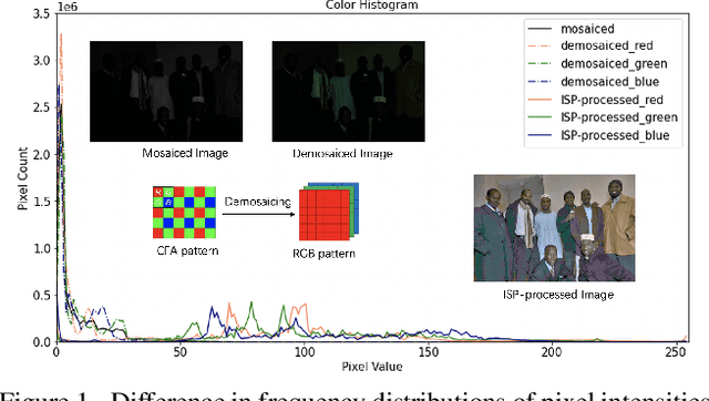
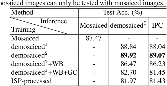
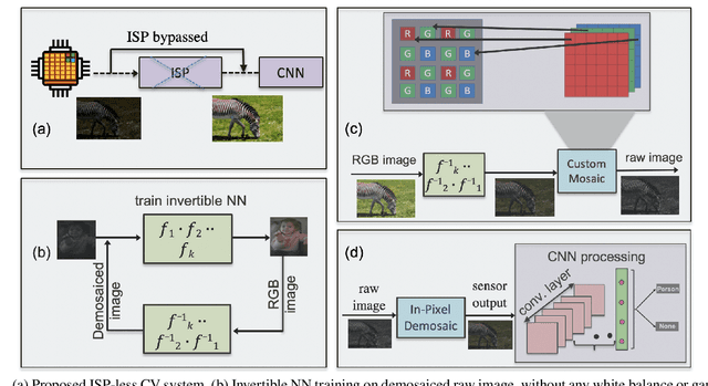
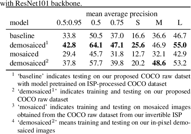
In order to deploy current computer vision (CV) models on resource-constrained low-power devices, recent works have proposed in-sensor and in-pixel computing approaches that try to partly/fully bypass the image signal processor (ISP) and yield significant bandwidth reduction between the image sensor and the CV processing unit by downsampling the activation maps in the initial convolutional neural network (CNN) layers. However, direct inference on the raw images degrades the test accuracy due to the difference in covariance of the raw images captured by the image sensors compared to the ISP-processed images used for training. Moreover, it is difficult to train deep CV models on raw images, because most (if not all) large-scale open-source datasets consist of RGB images. To mitigate this concern, we propose to invert the ISP pipeline, which can convert the RGB images of any dataset to its raw counterparts, and enable model training on raw images. We release the raw version of the COCO dataset, a large-scale benchmark for generic high-level vision tasks. For ISP-less CV systems, training on these raw images result in a 7.1% increase in test accuracy on the visual wake works (VWW) dataset compared to relying on training with traditional ISP-processed RGB datasets. To further improve the accuracy of ISP-less CV models and to increase the energy and bandwidth benefits obtained by in-sensor/in-pixel computing, we propose an energy-efficient form of analog in-pixel demosaicing that may be coupled with in-pixel CNN computations. When evaluated on raw images captured by real sensors from the PASCALRAW dataset, our approach results in a 8.1% increase in mAP. Lastly, we demonstrate a further 20.5% increase in mAP by using a novel application of few-shot learning with thirty shots each for the novel PASCALRAW dataset, constituting 3 classes.
P2M-DeTrack: Processing-in-Pixel-in-Memory for Energy-efficient and Real-Time Multi-Object Detection and Tracking
May 28, 2022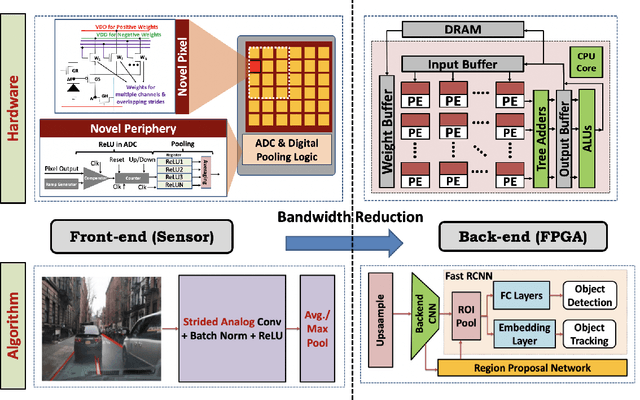
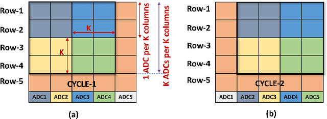
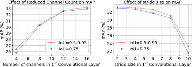
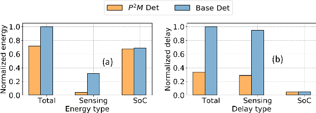
Today's high resolution, high frame rate cameras in autonomous vehicles generate a large volume of data that needs to be transferred and processed by a downstream processor or machine learning (ML) accelerator to enable intelligent computing tasks, such as multi-object detection and tracking. The massive amount of data transfer incurs significant energy, latency, and bandwidth bottlenecks, which hinders real-time processing. To mitigate this problem, we propose an algorithm-hardware co-design framework called Processing-in-Pixel-in-Memory-based object Detection and Tracking (P2M-DeTrack). P2M-DeTrack is based on a custom faster R-CNN-based model that is distributed partly inside the pixel array (front-end) and partly in a separate FPGA/ASIC (back-end). The proposed front-end in-pixel processing down-samples the input feature maps significantly with judiciously optimized strided convolution and pooling. Compared to a conventional baseline design that transfers frames of RGB pixels to the back-end, the resulting P2M-DeTrack designs reduce the data bandwidth between sensor and back-end by up to 24x. The designs also reduce the sensor and total energy (obtained from in-house circuit simulations at Globalfoundries 22nm technology node) per frame by 5.7x and 1.14x, respectively. Lastly, they reduce the sensing and total frame latency by an estimated 1.7x and 3x, respectively. We evaluate our approach on the multi-object object detection (tracking) task of the large-scale BDD100K dataset and observe only a 0.5% reduction in the mean average precision (0.8% reduction in the identification F1 score) compared to the state-of-the-art.
P2M: A Processing-in-Pixel-in-Memory Paradigm for Resource-Constrained TinyML Applications
Mar 17, 2022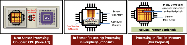
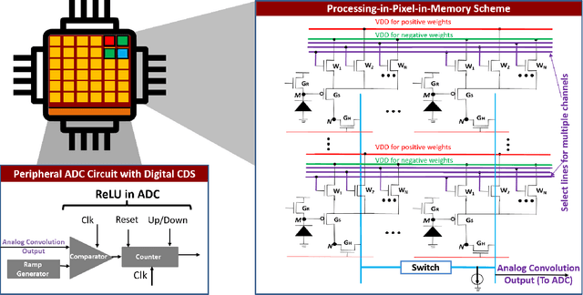
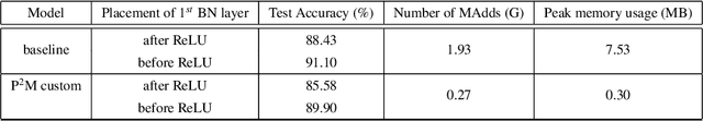
The demand to process vast amounts of data generated from state-of-the-art high resolution cameras has motivated novel energy-efficient on-device AI solutions. Visual data in such cameras are usually captured in the form of analog voltages by a sensor pixel array, and then converted to the digital domain for subsequent AI processing using analog-to-digital converters (ADC). Recent research has tried to take advantage of massively parallel low-power analog/digital computing in the form of near- and in-sensor processing, in which the AI computation is performed partly in the periphery of the pixel array and partly in a separate on-board CPU/accelerator. Unfortunately, high-resolution input images still need to be streamed between the camera and the AI processing unit, frame by frame, causing energy, bandwidth, and security bottlenecks. To mitigate this problem, we propose a novel Processing-in-Pixel-in-memory (P2M) paradigm, that customizes the pixel array by adding support for analog multi-channel, multi-bit convolution, batch normalization, and ReLU (Rectified Linear Units). Our solution includes a holistic algorithm-circuit co-design approach and the resulting P2M paradigm can be used as a drop-in replacement for embedding memory-intensive first few layers of convolutional neural network (CNN) models within foundry-manufacturable CMOS image sensor platforms. Our experimental results indicate that P2M reduces data transfer bandwidth from sensors and analog to digital conversions by ~21x, and the energy-delay product (EDP) incurred in processing a MobileNetV2 model on a TinyML use case for visual wake words dataset (VWW) by up to ~11x compared to standard near-processing or in-sensor implementations, without any significant drop in test accuracy.